
Organic EL display and method for manufacturing same

a technology of organic el and display, which is applied in the direction of discharge tube luminescnet screen, thermoelectric device, organic semiconductor device, etc., can solve the problems of air bubbles, poor light extraction efficiency, and reduced light extraction efficiency, so as to prevent the occurrence of luminance unevenness, the effect of filling defects of resin filler material

Active Publication Date: 2014-01-14
SHARP KK
View PDF7 Cites 5 Cited by
  • Summary
  • Abstract
  • Description
  • Claims
  • Application Information

AI Technical Summary

Benefits of technology

The invention provides an organic EL display with a color conversion panel that uses an inkjet method to form a color conversion layer. The panel includes barrier walls to guide the flow of resin filler material and prevent air bubbles when bonding the organic EL emission panel to the color conversion filter panel. This results in a better seal and prevents unevenness in luminance. The invention also provides a method for manufacturing the display without the need for an expensive high-precision mechanical measurement valve. Various dispenser methods, such as pneumatic pressure-control+syringe methods, can be used.

Problems solved by technology

As a result, the difference in refractive indexes of the filling gas or inert liquid and the constituent layers adjacent thereto is large, and so the efficiency of light extraction has not been very good.
At the portions of the air bubbles 500, the efficiency of light extraction is reduced due to the difference in refractive index, and luminance unevenness results.
Also, as shown in FIG. 3, air bubbles 500 occurring in dropped portions cannot be adequately removed in vacuum due to the high viscosity of the resin filler material, and may expand and spread considerably during evacuation and during heating and hardening of the resin filler material.
Further, in methods of bonding by dropping a general liquid filler material in vacuum, adopted in bonding of liquid crystals and similar, the liquid filler material does not spread uniformly to the corners of the screen region, and there are cases in which luminance unevenness and similar occur.
However, the resistance of the barrier walls 221 is considerable, and a large amount of time is required for the liquid filler material to spread to the corners of the screen region.

Method used


Image

  • Organic EL display and method for manufacturing same
  • Organic EL display and method for manufacturing same
  • Organic EL display and method for manufacturing same

Examples


example 1

Practical Example 1

Organic EL Emission Panel 10

[0153]TFT structures 102 for a plurality of screen portions were formed on an alkali-free glass substrate 100 of 200×200 mm×0.7 mm thick (product name AN-100, manufactured by Asahi Glass Co., Ltd.), the TFT structures 102 were covered with a planarization layer 103 comprising a resin layer of thickness 3 μm and an SiO2 passivation layer of thickness 300 nm, and contact holes penetrating the planarization layer 103 and SiO2 passivation layer were formed, to prepare an organic EL emission panel substrate 100.

[0154]A sputtering device (RF-planar magnetron) was used to deposit an IZO film of thickness 50 nm onto the organic EL emission panel substrate 100 in an Ar gas atmosphere, a resist (product name OFRP-800, manufactured by Tokyo Ohka Kogyo Co., Ltd.) was applied thereto, exposure and development were performed to form a pattern, and by performing wet etching, an underlayer 110 was formed, separated into island shapes at each subpixel. ...

example 2

Practical Example 2

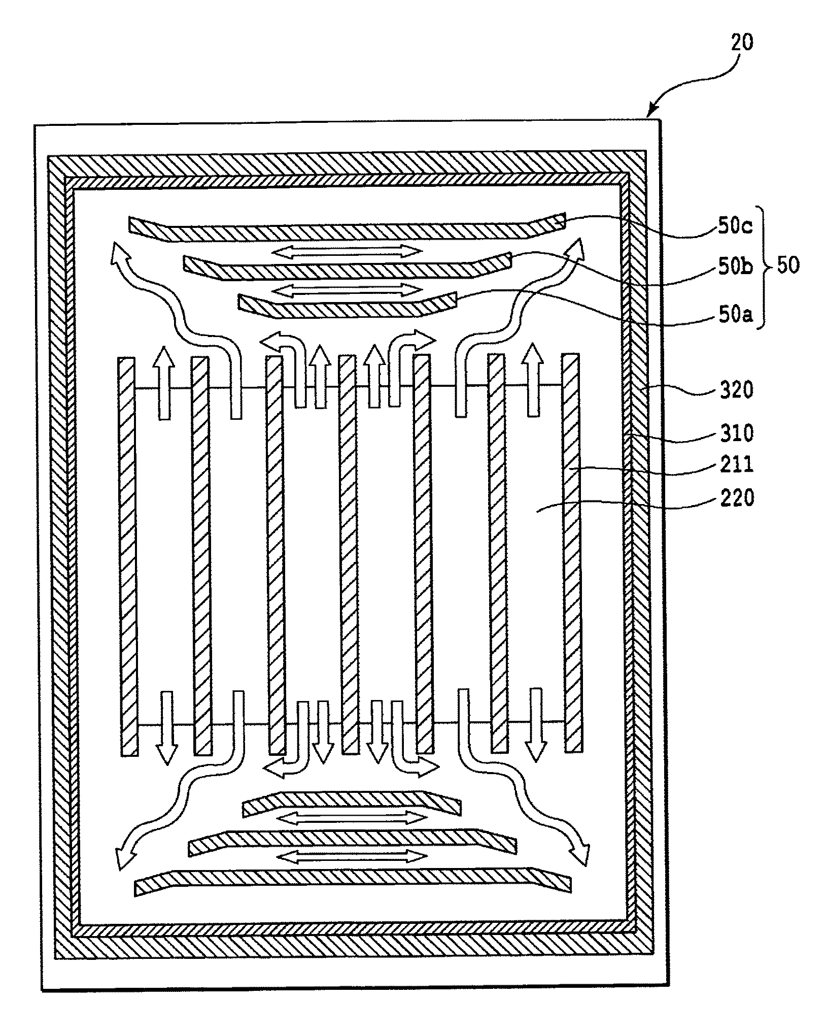
[0179]Processing similar to that of Practical Example 1 was performed to simultaneously manufacture a plurality of organic EL displays except for, during manufacture of the color conversion filter panels 20 in Practical Example 1 above, dividing the filler material guide wall 50 into five equal portions and arranging them intermittently at intervals of approximately 1 mm as shown in FIG. 4, and placing the thermosetting type adhesive 40 at multiple points as shown in FIG. 18 when bonding together the organic EL emission panels 10 and the color conversion filter panels 20.

[0180]In this practical example, satisfactory organic EL displays similar to those of Practical Example 1 were obtained.

example 3

Practical Example 3

[0181]Except for forming filler material guide walls 50 having bent portions, and using a resin filler material with a viscosity of from 200 to 500 mPa·s, processing similar to that of Practical Example 1 was performed, to simultaneously manufacture a plurality of organic EL displays.

[0182]The resin material guide walls 50 were formed in three rows with a pitch of 180 μm, taking an interval of approximately 1.5 mm from both tip portions of the barrier walls for inkjet application 221. Each of the rows of filler material guide walls 50 had a width of 14 μm and a height of 5 μm. The rows of filler material guide walls 50 had lengths, in order from the side of the barrier walls for inkjet application 221, of 15 mm, 22 mm, and 35 mm. And, bent portions of length 5 mm were formed from both ends of each of the rows of the filler material guide walls 50, with each of the bent portions directed in the direction of the closest corner of the peripheral seal wall 310.

[0183]I...


PUM


Abstract

An object of this invention is to provide a top-emission type organic EL display in which filling defects of a resin filler material are alleviated during bonding of an organic EL emission panel and a color conversion filter panel with the resin filler material, as well as to provide a method for manufacturing such an organic EL display. An organic EL display of this invention is characterized in having stripe-shaped barrier walls for inkjet application placed on a color conversion filter panel, and a filler material guide wall placed between the length-direction end portions of the barrier walls for inkjet application and a peripheral seal member.

Description

TECHNICAL FIELD[0001]This invention relates to an organic EL display. More specifically, this invention relates to a top-emission type organic EL display formed by an organic EL emission panel, and a color conversion filter panel which receives light in a prescribed wavelength range emitted by the organic EL emission panel, converts the light to light in the wavelength range of the desired chromaticity, and emits the light to a screen, as well as to the structure of the color conversion filter panel.BACKGROUND ART[0002]Organic EL displays known in the prior art include bottom-emission type displays, in which an organic EL emission panel is formed directly on a color conversion filter panel, and top-emission type displays, in which a separately manufactured color conversion filter panel and organic EL emission panel are bonded together, with the emission region of the organic EL emission panel and the color pattern formation region of the color conversion filter panel opposed, and wi...

Claims


Application Information

Patent Timeline
Patent Type & Authority Patents(United States)
IPC IPC(8): H01J33/00
CPCH01L51/5237H01L27/322H05B33/02H01L2251/5315H10K59/38H10K2102/3026H10K59/8731H10K59/8723H10K59/8722H10K59/80518H10K50/11H10K2102/00H10K50/8426H10K50/8428H10K50/8445
Inventor NAKAMURA, HIDEYOHASHIMOTO, KOHICHI
Owner SHARP KK
Learn More