Semiconductor laser drive device and image forming apparatus incorporating same

a technology of semiconductor laser and drive device, which is applied in the direction of semiconductor laser, electrographic process, instruments, etc., can solve the problems of semiconductor laser degradation, semiconductor laser degradation, and semiconductor laser degradation

Inactive Publication Date: 2014-01-14
RICOH KK
View PDF15 Cites 0 Cited by
  • Summary
  • Abstract
  • Description
  • Claims
  • Application Information

AI Technical Summary

Benefits of technology

[0060]As described above, the semiconductor laser drive device 7 according to the first embodiment includes the A / D conversion unit that converts the current value (analog value) to the digital value. Accordingly, the image controller 6 does not need to include an A / D conversion unit. Consequently, it becomes possible to detect the degradation of the semiconductor laser LD without complication, expansion and cost increase of the image controller 6.
[0061]The signal representing the detected value of the drive current Iop, that is, the current control signal opdet_dac [7:0] is generated as the digital value, and is output. Accordingly, using this digital value of the drive current Iop, the degradation of the semiconductor laser LD can be detected with a high degree of accuracy in the image controller 6.
[0062]Thus, the semiconductor laser drive device 7 according to the first embodiment can perform the degradation detection of the semiconductor laser LD with a high degree of accuracy, and it is also possible to avoid complication, expansion and cost increase of the image controller 6.
[0070]The storage circuit 18 stores the value of the current control signal opdet_dac [7:0] representing the abnormal level of the drive current Iop that is the criterion for determining the degradation of the semiconductor laser LD as the digital value. The second comparator 22 and the NMOS transistor Tr1 function as an abnormality detection circuit (degradation detector) that detects a current value of the drive current Iop supplied to the semiconductor laser LD to emit light at a predetermined intensity and generates an abnormality detection signal err indicating the abnormal state for output when the value of the current control signal opdet_dac [7:0] as the detected current value exceeds the threshold signal err_code[7:0] representing the abnormal level of the drive current Iop. In the drive current detection circuit, the PMOS transistor Trm functions as a proportional current generator, the D / A converter 12 functions as a D / A conversion circuit, and the counter 15 functions as a counter circuit.
[0059]In this configuration, even when the semiconductor laser LD degrades due to above-described factors, it is possible to determine the degradation of the semiconductor laser LD easily by detecting the increase of the drive current Iop necessary to obtain a desired quantity of light.

Problems solved by technology

However, the semiconductor laser degrades due to various factors.
More specifically, degradation of the semiconductor laser may arise due to crystal defect within several hours.
Further, the degradation of the semiconductor laser may arise gradually by being driven at high temperature for a long time.
Further, the degradation of the semiconductor laser may arise due to catastrophic optical damage (COD) or an electrostatic discharge (ESD) during assembly of the laser printers and the digital copiers.
When the drive current is increased excessively and power consumption exceeds a rated value, the semiconductor laser may degrade due to heat generated by the power and cause trouble.
Further, when a large current beyond the assumed value flows from a semiconductor laser drive device, there is also a possibility of a defect arising due to melting of metal wiring.
However, when the value of drive current Iop is small and below a predetermined current value, the signal indicating abnormality may not be output in the semiconductor laser drive device shown in FIG. 1.
However, the semiconductor laser drive device shown in FIG. 2 outputs an analog value, making it necessary to mount an analog-to-digital (A / D) converter that converts an analog value to a digital value on the circuit board or have a built-in circuit in the image controller because the image controller cannot perform data processing with the analog value directly.
Consequently, the configuration of the image controller becomes complicated and the chip area of the image controller expands, resulting in a cost penalty.

Method used


Image

  • Semiconductor laser drive device and image forming apparatus incorporating same
  • Semiconductor laser drive device and image forming apparatus incorporating same
  • Semiconductor laser drive device and image forming apparatus incorporating same

Examples


first embodiment

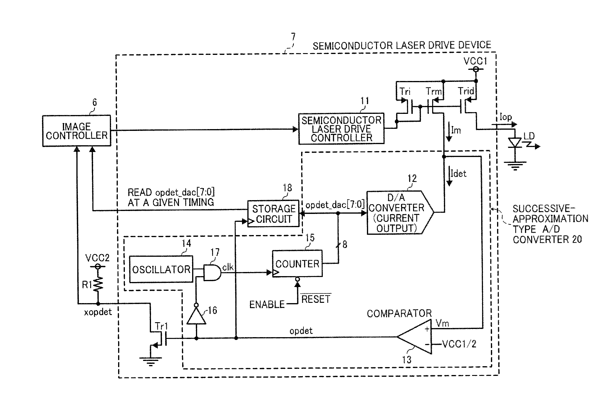
[0036]FIG. 5 is a circuit diagram of the semiconductor laser drive device 7 according to a In FIG. 5, the semiconductor laser drive device 7 includes PMOS transistors Tri, Trm, and Trld, a semiconductor-laser drive controller 11, a digital to analog converter (hereinafter “D / A converter”) 12, a comparator 13, and an NMOS transistor Tr1. The PMOS transistors Tri, Trm, and Trld constitute a current mirror circuit. The semiconductor-laser drive controller 11 controls gate voltages of the PMOS transistors Tri, Trm, and Trld in accordance with the control signal input from the image controller 6. The D / A converter 12 is a current output type converter that generates a detection current Idet having a current value according to 8 bit current control signal opdet_dac [7:0] and outputs the detection current Idet.

[0037]Further, the semiconductor laser drive device 7 includes an oscillator 14, a counter 15, an inverter 16, an AND circuit 17, and a storage circuit 18. The oscillator 14 generat...

second embodiment

[0064](Second Embodiment)

[0065]A semiconductor laser drive device 7b according to an illustrative second embodiment is described below with reference to FIGS. 7 through 8B.

[0066]FIG. 7 is a circuit diagram of the semiconductor laser drive device 7b according to the second embodiment. It is the difference between the semiconductor laser drive device of FIG. 7 and that of FIG. 5 that the semiconductor laser drive device 7b includes a nonvolatile memory 21 and a second comparator 22. The nonvolatile memory 21 stores a threshold signal err_code[7:0] representing an abnormal level of the drive current Iop that is one criterion for determining the degradation of the semiconductor laser LD as a digital value. The second comparator 22 compares the value of the signal opdet_dac[7:0] representing the detected drive current Iop with the value of the threshold signal err_code[7:0] representing the abnormal level of the drive current Iop. Similarly to the first embodiment, a current control sign...

third embodiment

[0089]However, in the semiconductor laser drive device that includes more than one D / A converters, all the currents generated by each D / A converter may be added to supply it to the semiconductor laser LD. In such a semiconductor laser drive device, it is sufficient to calculate and add the control code of each D / A converter to obtain the desired function to output. Such a semiconductor laser drive device is proposed as a

[0090](Third Embodiment)

[0091]A semiconductor laser drive device 7c according to an illustrative third embodiment is described with reference to FIG. 9.

[0092]FIG. 9 is a circuit diagram of the semiconductor laser drive device 7c according to the third embodiment. In the embodiment shown in FIG. 9, the semiconductor laser drive device 7c includes a drive circuit 30 that includes three D / A converters including a first DAC 31, a second DAC 32, and a third DAC 33, and a controller 34. The drive circuit 30 supplies a drive current Iop to the semiconductor laser LD by addi...


PUM


Abstract

A semiconductor laser drive device includes a semiconductor-laser drive element to generate a drive current according to an input control signal to supply the drive current to a semiconductor laser, a control circuit to control the drive current by controlling the semiconductor-laser drive element, and a drive current detection circuit to detect a current value of the drive current supplied to the semiconductor laser and generate a digital control signal representing the detected digital value of the drive current to output.

Description

TECHNICAL FIELD[0001]The present disclosure relates to a semiconductor laser drive device, and more particularly, to a semiconductor laser drive device capable of detecting degradation of a semiconductor laser with a high degree of accuracy with an uncomplicated configuration.BACKGROUND ART[0002]Recently, semiconductor laser diodes (hereinafter, referred to as “semiconductor laser”) have come to be widely used in a variety of image forming apparatuses using electrophotography, for example, laser printers and digital copiers.[0003]However, the semiconductor laser degrades due to various factors. More specifically, degradation of the semiconductor laser may arise due to crystal defect within several hours. Further, the degradation of the semiconductor laser may arise gradually by being driven at high temperature for a long time.[0004]Further, the degradation of the semiconductor laser may arise due to catastrophic optical damage (COD) or an electrostatic discharge (ESD) during assembl...

Claims


Application Information

Patent Timeline
Patent Type & Authority Patents(United States)
IPC IPC(8): B41J2/435H01S3/10
CPCG03G15/04072H01S5/06808H01S3/10H01S5/06
Inventor SUMINO, DAIJIROHKYOGOKU, HIROAKI
Owner RICOH KK
Why Eureka
Try Eureka