Polishing pad seasoning method, seasoning plate, and semiconductor polishing device

a technology of semiconductor polishing and polishing pad, which is applied in the direction of grinding drive, grinding drive, abrasive surface conditioning device, etc., can solve the problems of reducing the polishing efficiency of wafers, deteriorating polishing pads, and difficult to form minute circuit patterns, so as to prevent the appearance of inflection points in the pad surface of polishing pads due to conditioners and achieve uniform variations in polishing pads. , the effect of simple structur

Active Publication Date: 2014-03-04
SUMCO TECHXIV
View PDF21 Cites 0 Cited by
  • Summary
  • Abstract
  • Description
  • Claims
  • Application Information

AI Technical Summary

Benefits of technology

[0016]In view of the above problems, the present invention aims to provide a seasoning method, a seasoning plate, and a semiconductor polishing device that can recover the flatness of a polishing pad with a simple structure, and can readily control the flatness of the polished surface by adjusting the rotation speed of the polishing pad.
[0018]A second aspect of the polishing pad seasoning method according to the present invention is characterized as a polishing pad seasoning method for abrading a polishing pad by the friction caused by rotation of the polishing pad, the method including: attaching conditioners for abrading the polishing pad to the lower face of a round flexible substrate; mounting a weight portion on the upper face of the flexible substrate, to press the conditioners against the polishing pad; and applying weight for deforming the flexible substrate to the flexible substrate by a ring placed between the flexible substrate and the weight portion, to eliminate inflection points in the pad surface of the polishing pad, the inflection points appearing during the abrasion of the polishing pad by the conditioners, the ring forming a circle concentric with the flexible substrate.
[0031]A second aspect of the semiconductor polishing device according to the present invention is characterized as a semiconductor polishing device on which a seasoning plate can be mounted, the seasoning plate being placed on a polishing pad and performing seasoning of the polishing pad by abrading the polishing pad through the friction caused by rotation of the polishing pad, the seasoning plate including: conditioners that abrade the polishing pad; a round flexible substrate that has the conditioners attached to the lower face thereof; a weight portion that applies weight to the flexible substrate; and a ring that is placed between the flexible substrate and the weight portion, and applies weight for deforming the flexible substrate to the flexible substrate, the ring forming a circle concentric with the flexible substrate, the ring eliminating inflection points in the pad surface of the polishing pad, the inflection points appearing during the abrasion of the polishing pad by the conditioners.
[0039]With the polishing pad seasoning method, the seasoning plate, and the semiconductor polishing device according to the present invention, the variations in abrasion depth in the inner circumferential region and the outer circumferential region of polishing pad can be reduced with a simple structure, while using conventional conditioners. Also, appearance of inflection points in the pad surface of the polishing pad due to the conditioners can be prevented, and the variations in abrasion depth of the polishing pad can be made uniform. In this manner, the flatness of the polished surface can be readily maintained by controlling the rotation speed of the polishing pad. Thus, the duration of use (the life) of the polishing pad can be prolonged, and costs can be lowered.

Problems solved by technology

However, if the surface flatness of the wafer manufactured through the above-described procedures is low, part of the lens used in the exposure in a photolithography process for forming circuits does not come into focus, and it becomes difficult to form a minute circuit pattern.
Since chips generated during polishing operations and slurry abrasive grains remain on the polishing pad, the polishing pad deteriorate, and the wafer polishing efficiency drops rapidly, as the wafer polishing operations continue.
As a result, the slurry does not spread evenly on the polishing pad, and this phenomenon causes variations of wafer surface polishing conditions and a decrease in wafer polishing removal efficiently.
When a silicon wafer is polished with the use of a polishing pad having a shape represented by such a convex curve, the flatness of the surface of each silicon wafer becomes poorer, and more polishing is performed on the side of the silicon wafer positioned in the inner circumferential region of the polishing pad than on the side of the silicon wafer positioned in the outer circumferential region of the polishing pad.
However, when the rotation speed becomes lower, the polishing efficiency also becomes lower.
However, depending on the surface condition of the polishing pad, a silicon wafer might have either inner abrasion or outer abrasion, even if the polishing pad is rotated at a fixed rotation speed.
Therefore, it is difficult to control the flatness of the polished surface of each silicon wafer by adjusting the rotation speed of the polishing pad.
As a result, the structure becomes complicated, and the costs become higher.
However, unlike a conventional ring-like conditioner, the conditioner 300 has a complicated structure, resulting in higher costs.

Method used


Image

  • Polishing pad seasoning method, seasoning plate, and semiconductor polishing device
  • Polishing pad seasoning method, seasoning plate, and semiconductor polishing device
  • Polishing pad seasoning method, seasoning plate, and semiconductor polishing device

Examples


Embodiment Construction

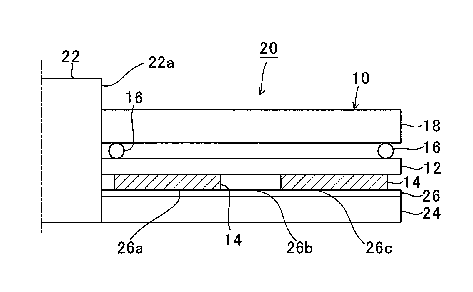
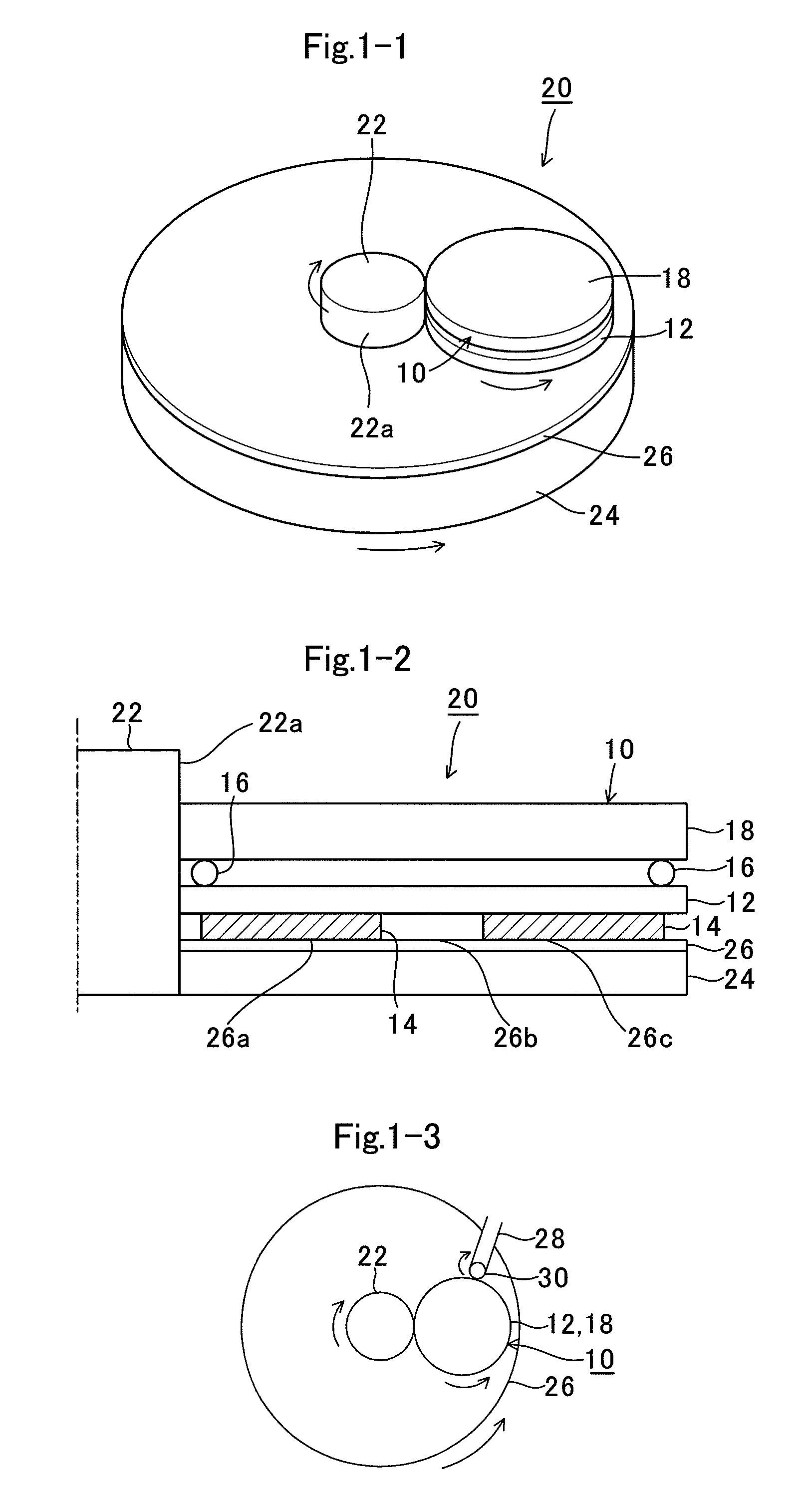
[0065]The following is a description of an embodiment of a polishing pad seasoning method, a seasoning plate, and a semiconductor polishing device according to the present invention, with reference to the accompanying drawings. The components and the types, combinations, shapes, and relative positions of the components described in the embodiment are merely examples and do not restrict the scope of the invention to those examples, unless otherwise specified.

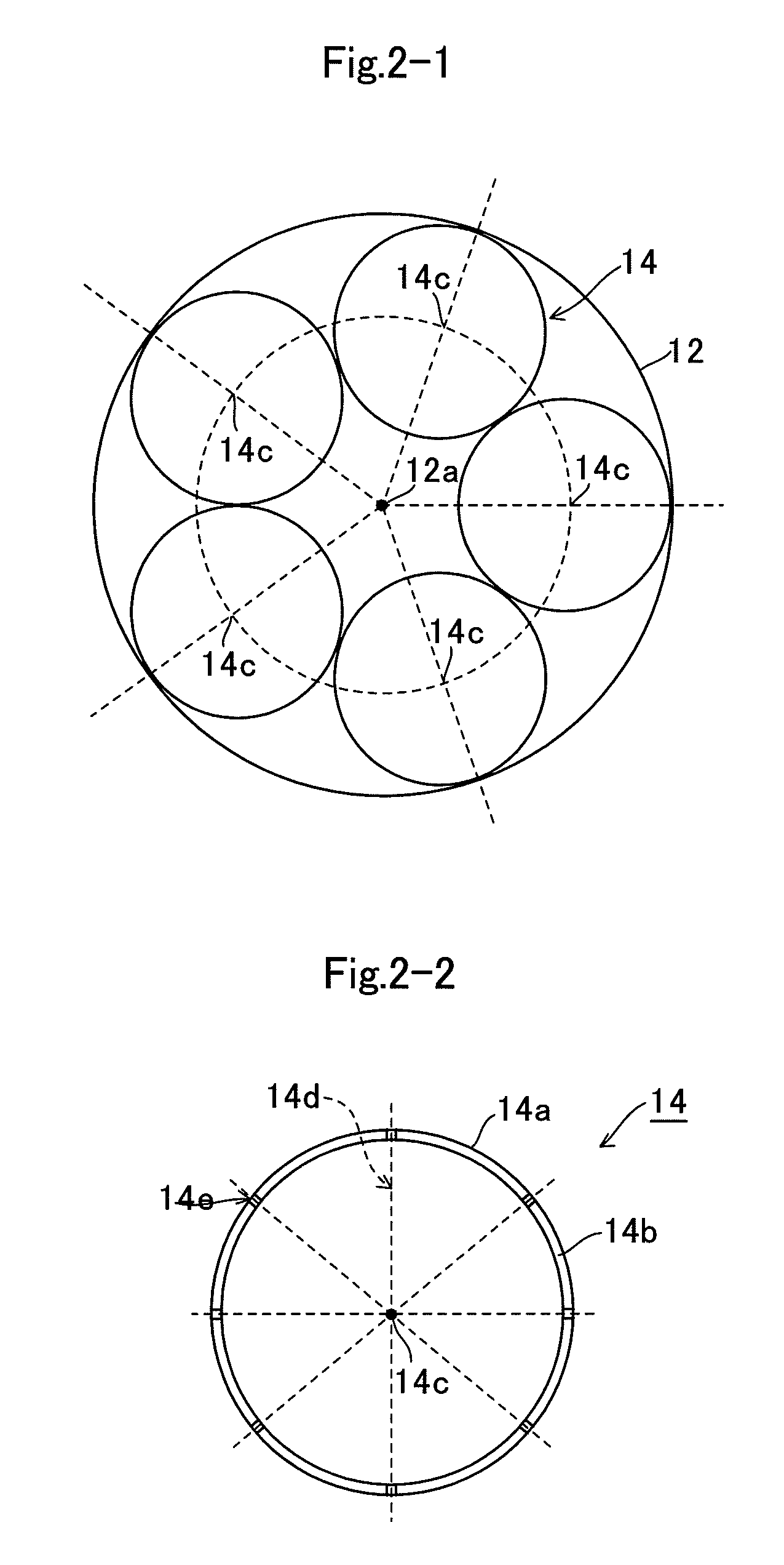
[0066]FIG. 1-1 is a perspective view of a seasoning plate and a semiconductor polishing device according to this embodiment. FIG. 1-2 is a partial cross-sectional view of the structures shown in FIG. 1-1, and FIG. 1-3 is a plan view of the structures shown in FIG. 1-1. By a polishing pad seasoning method according to this embodiment, a polishing pad is ground by the friction caused by rotating the polishing pad. Conditioners for grinding the polishing pad are attached to the bottom face of a round flexible substrate, and a ring t...


PUM

PropertyMeasurementUnit
frictionaaaaaaaaaa
flexibleaaaaaaaaaa
weightaaaaaaaaaa

Abstract

A seasoning plate is placed on a polishing pad and performs seasoning of the polishing pad by abrading the polishing pad through the friction caused by rotation of the polishing pad. The seasoning plate includes: conditioners that abrade the polishing pad; a round flexible substrate that has the conditioners attached to the lower face thereof; an O-ring that is placed on the upper face of the flexible substrate, the O-ring forming a circle concentric with the flexible substrate; and a weight plate serving as a weight portion that is placed on the O-ring and applies weight for deforming the flexible substrate.

Description

BACKGROUND[0001](a) Field of the Invention[0002]The present invention relates to a semiconductor polishing technique, and more particularly, to a semiconductor polishing technique by which a semiconductor wafer is brought into contact with a polishing pad.[0003](b) Description of the Related Art[0004]Conventionally, a material wafer for manufacturing a semiconductor device is formed by growing a single-crystal semiconductor ingot of silicon or the like by the Czochralski method (CZ method) or the floating zone method (FZ method), abrading and shaping the outer periphery of the semiconductor ingot with the use of a cylindrical grinding machine or the like, and slicing the semiconductor ingot with a wire saw in a slicing process. After that, chamfering is performed on the wafer peripheral portions, and flattening and etching are also performed in a wrapping process. Primary polishing (rough polishing) and secondary polishing (finishing) are then performed to form a mirror wafer.[0005]...

Claims


Application Information

Patent Timeline
Patent Type & Authority Patents(United States)
IPC IPC(8): H01L21/304B24B53/017B24B1/00B24B53/12
CPCB24B53/017
Inventor MARUOKA, DAISUKEMOROIWA, KOUDAI
Owner SUMCO TECHXIV
Why Eureka
Try Eureka