
Semiconductor device including a circuit configured to hold an offset voltage

a technology of offset voltage and semiconductor device, which is applied in the direction of pulse generator, pulse technique, instruments, etc., can solve the problems of promoting degradation of transistors, affecting the operation of pulse generators, so as to reduce the vgs of transistors, prevent circuit malfunction, and reduce the drain current of transistors in the off-state

Active Publication Date: 2014-04-15
SEMICON ENERGY LAB CO LTD
View PDF15 Cites 14 Cited by
  • Summary
  • Abstract
  • Description
  • Claims
  • Application Information

AI Technical Summary

Benefits of technology

The present invention aims to provide a semiconductor device that can operate stable even when a transistor it contains is a depletion transistor. It also aims to decrease degradation of the transistor to prevent malfunction of a circuit. The invention achieves this by reducing the drain current of the transistor when it is off-state and suppressing the decrease in Vgs, which slows down degradation of the transistor.

Problems solved by technology

When the gate of the transistor M1 cannot be made into the floating state, the bootstrap operation cannot be performed normally, which may lead to malfunction or narrowing of the operating frequency range.
Further, in the case where the signal at low level is output as the signal OUT, since the driving voltage of the driver circuit of a display device is high, Vgs of the transistor M2 and the transistor M3 are also large, which promotes degradation of the transistors and may cause malfunction of the driver circuit.

Method used


Image

  • Semiconductor device including a circuit configured to hold an offset voltage
  • Semiconductor device including a circuit configured to hold an offset voltage
  • Semiconductor device including a circuit configured to hold an offset voltage

Examples


embodiment 1

(Embodiment 1)

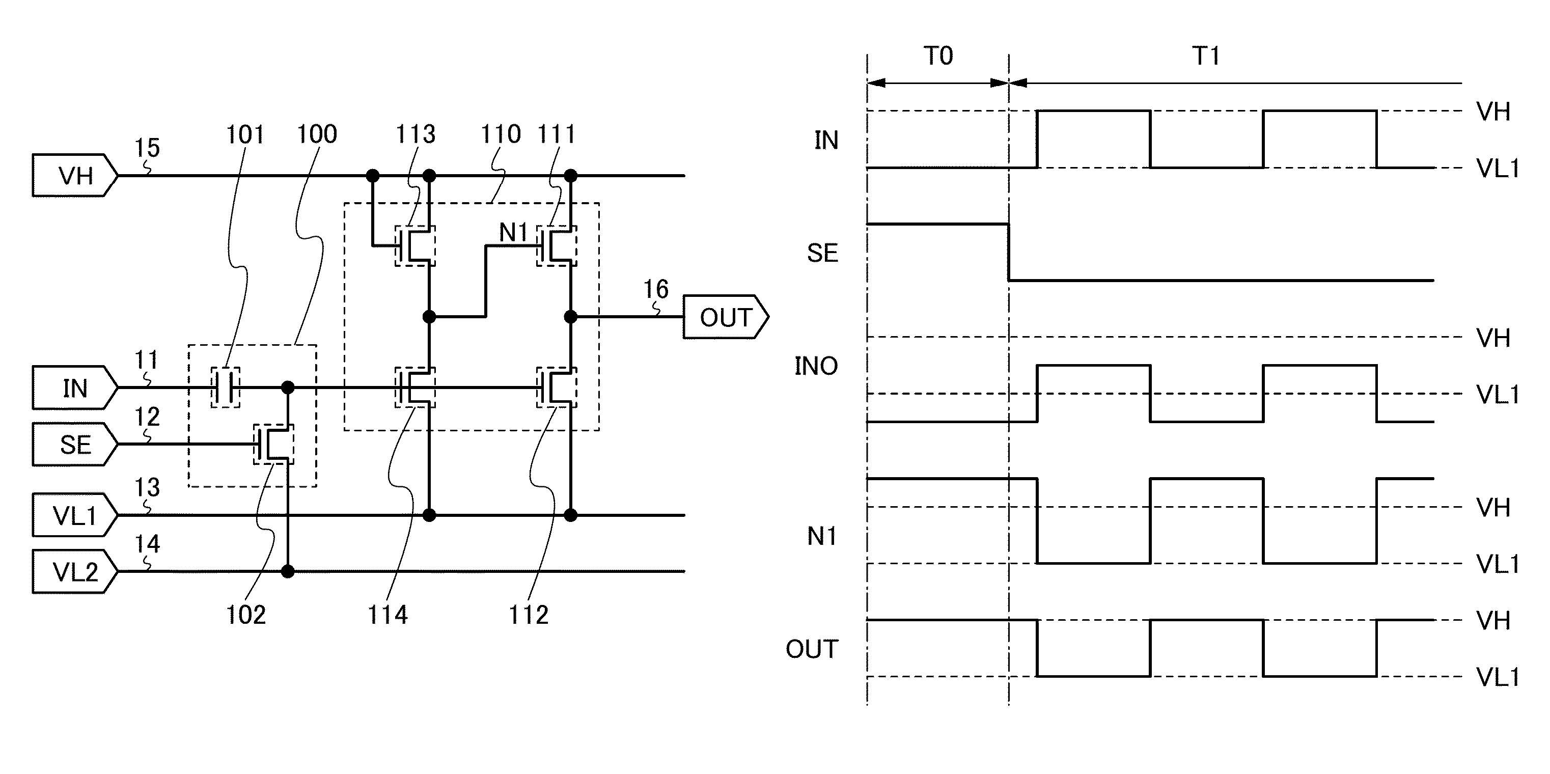
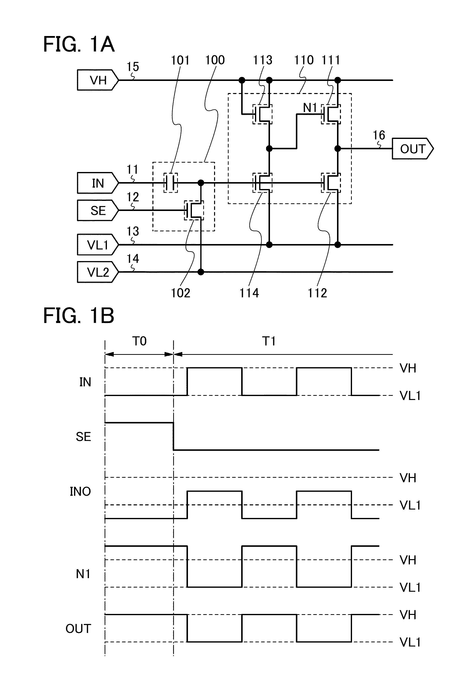
[0039]In this embodiment, one example of a semiconductor device which is driven by a signal generated by offsetting an input signal is described.

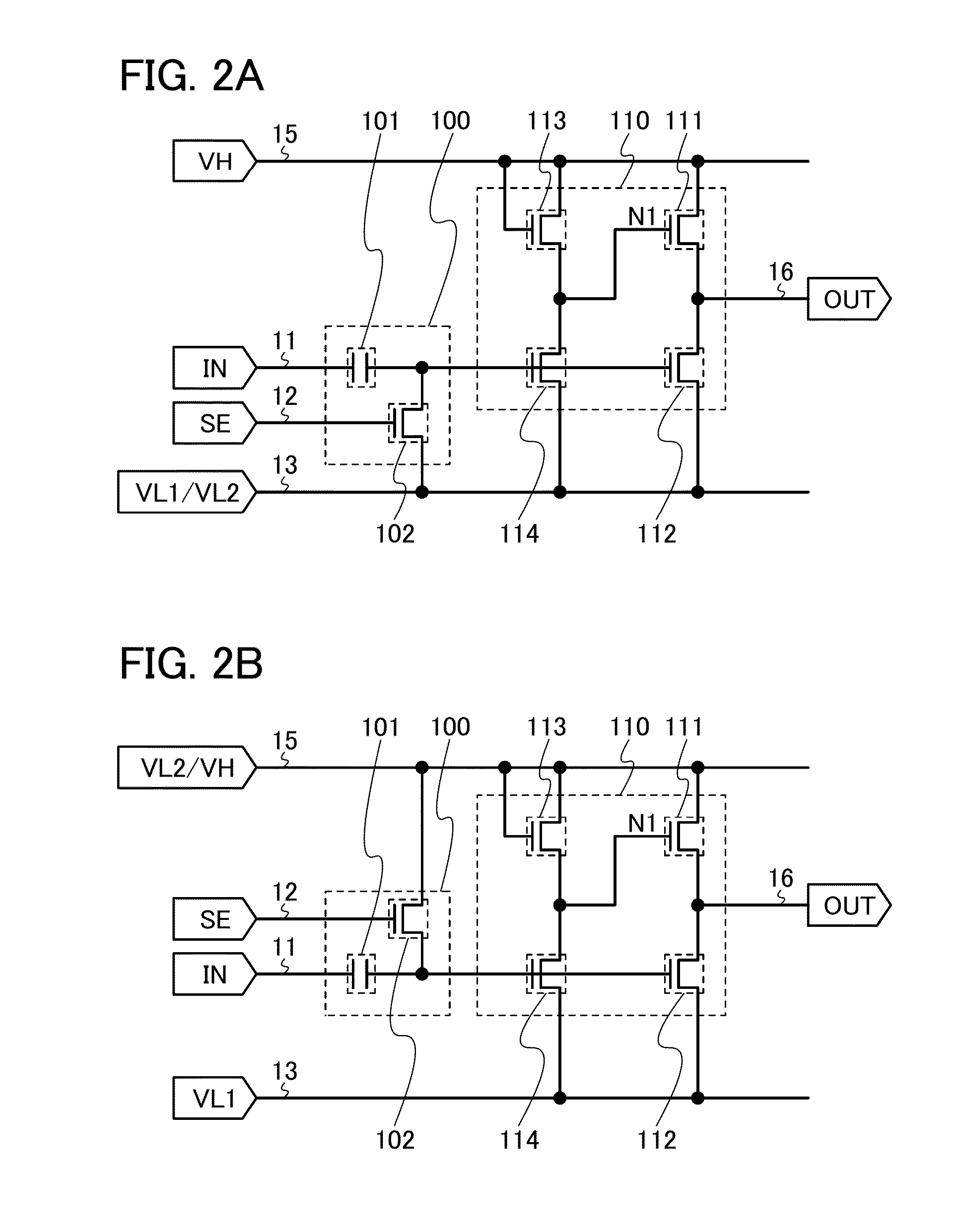
[0040]A configuration of a semiconductor device of this embodiment is described with reference to FIG. 1A. FIG. 1A is a circuit diagram of the semiconductor device of this embodiment. The semiconductor device in FIG. 1A includes a circuit 100 and a circuit 110. The circuit 100 is connected to a wiring 11, a wiring 12, a wiring 14, and the circuit 110. The circuit 110 is connected to a wiring 15, a wiring 13, a wiring 16, and the circuit 100. The wirings and the like connected to any of the circuits 100 and 110 can be changed as appropriate depending on the configurations of the circuits 100 and 110.

[0041]Note that in this specification, the case where X and Y are electrically connected to each other, the case where X and Y are functionally connected to each other, and the case where X and Y are directly connected to each other...

embodiment 2

(Embodiment 2)

[0110]In this embodiment, the case where the semiconductor device which is one embodiment of the present invention is used for a flip-flop circuit included in a shift register is described. Description is made on portions different from Embodiment 1.

[0111]The semiconductor device of this embodiment is described with reference to FIG. 6A. FIG. 6A is a circuit diagram of the semiconductor device of this embodiment. The semiconductor device in FIG. 6A is different from that shown in FIG. 1A in that the first terminal of the transistor 111 is connected to a wiring 23, the gate of the transistor 113 is connected to a wiring 21, and the one electrode of the capacitor 101 is connected to a wiring 22.

[0112]Signal IN1 is input to the wiring 21. The signal IN1 is an input signal of the semiconductor device and serves as a start pulse. For example, the signal IN1 is a digital signal whose high-level potential is VH and low-level potential is VL1. The wiring 21 transmits the signa...

embodiment 3

(Embodiment 3)

[0158]In this embodiment, a shift register in which the semiconductor device described in Embodiment 2 is used as a flip-flop circuit is described. Description is made on portions different from Embodiments 1 and 2.

[0159]The shift register of this embodiment is described with reference to FIG. 11. FIG. 11 is a circuit diagram of the shift register of this embodiment. The shift register in FIG. 11 includes N flip-flop circuits 200 (N is a natural number). Among these, 1st to 3rd stage flip-flop circuits 200 (denoted by a flip-flop circuit 200_1, a flip-flop circuit 200_2, and a flip-flop circuit 200_3) are shown in FIG. 11.

[0160]In the shift register shown in FIG. 11, the semiconductor device shown in FIG. 6A is used as the flip-flop circuit 200. However, the flip-flop circuit 200 is not limited to the semiconductor device shown in FIG. 6A and any other semiconductor device described in Embodiment 2 can be used as appropriate.

[0161]Connection relations in the shift regi...


PUM

PropertyMeasurementUnit
specific resistivityaaaaaaaaaa
Raaaaaaaaaaa

Abstract

Provided is a semiconductor device which can operate stably even in the case where a transistor thereof is a depletion transistor. The semiconductor device includes a first transistor for supplying a first potential to a first wiring, a second transistor for supplying a second potential to the first wiring, a third transistor for supplying a third potential at which the first transistor is turned on to a gate of the first transistor and stopping supplying the third potential, a fourth transistor for supplying the second potential to the gate of the first transistor, and a first circuit for generating a second signal obtained by offsetting a first signal. The second signal is input to a gate of the fourth transistor. The potential of a low level of the second signal is lower than the second potential.

Description

BACKGROUND OF THE INVENTION[0001]1. Field of the Invention[0002]One embodiment of the present invention relates to semiconductor devices and display devices.[0003]2. Description of the Related Art[0004]Display devices with higher value have been developed accompanying spread of large-sized display devices such as liquid crystal television. In particular, a technology of using transistors whose conductivity types are the same as each other in a driver circuit has been actively developed (see Patent Document 1).[0005]FIG. 23 illustrates a driver circuit described in Patent Document 1. The driver circuit described in Patent Document 1 includes transistors M1, M2, M3, and M4 and a capacitor C1. In Patent Document 1, in the case where a signal at high level is output as a signal OUT, a gate of the transistor M1 is made into a floating gate, and a bootstrap operation in which the potential of the gate of the transistor M1 is increased to be higher than a potential VDD by using capacitive ...

Claims


Application Information

Patent Timeline
Patent Type & Authority Patents(United States)
IPC IPC(8): G05F1/10G02F1/167
CPCG11C19/28G09G2320/043H03K19/018521G09G3/20G11C19/184G09G2330/021H03K17/08104G09G2310/0286H10K59/12G09G3/36H01L27/1214H03K19/01714G09G3/3688H03K3/356G09G2300/0819G09G2300/0876G09G2300/0426G02F1/167H03K17/06G02F1/1368G09G3/3225G09G3/344G09G3/3648H01L27/1225H01L27/124H01L27/1255H01L29/7869
Inventor UMEZAKI, ATSUSHI
Owner SEMICON ENERGY LAB CO LTD
Learn More