Solid-state imaging device comprising an analog to digital converter with column comparison circuits, column counter circuits, first and second inverters, and buffers

a technology of solid-state imaging and analog to digital converter, which is applied in the direction of code conversion, instruments, television systems, etc., can solve the problems of greater generated noise, achieve the effect of reducing the duty of the clock, facilitating the extension of the ad conversion bit width, and high accuracy

Active Publication Date: 2014-05-27
PANASONIC SEMICON SOLUTIONS CO LTD
View PDF37 Cites 11 Cited by
  • Summary
  • Abstract
  • Description
  • Claims
  • Application Information

AI Technical Summary

Benefits of technology

[0048]With the solid-state imaging device and the imaging device according to the present invention, in a MOS-type solid-state imaging device equipped with a ramp-type AD converter, a clock signal for a counter (a count clock) can be supplied to each of the column AD converter while the waveform of the clock signal for count is maintained at high accuracy (a decrease in the duty of the clock is restricted). Therefore, it is easier to realize extension of AD conversion bit width and an increase in the number of pixels that directly connect to improvement of image quality of still images, and it is possible to increase a frame rate and to obtain smoother moving images.
[0049]Furthermore, the number of clock buffer stages can be two stages (only the first stage and the second stage) regardless of the number of columns of column AD converters and therefore an increase in the layout area can be restricted, while by providing dedicated power source and GND wiring to each of the clock buffer stages and by adding decoupling capacity, peak current and an increase in noise caused by the peak current can be restricted.

Problems solved by technology

When an operating frequency is higher, generated noise is greater.

Method used


Image

  • Solid-state imaging device comprising an analog to digital converter with column comparison circuits, column counter circuits, first and second inverters, and buffers
  • Solid-state imaging device comprising an analog to digital converter with column comparison circuits, column counter circuits, first and second inverters, and buffers
  • Solid-state imaging device comprising an analog to digital converter with column comparison circuits, column counter circuits, first and second inverters, and buffers

Examples


embodiment 1

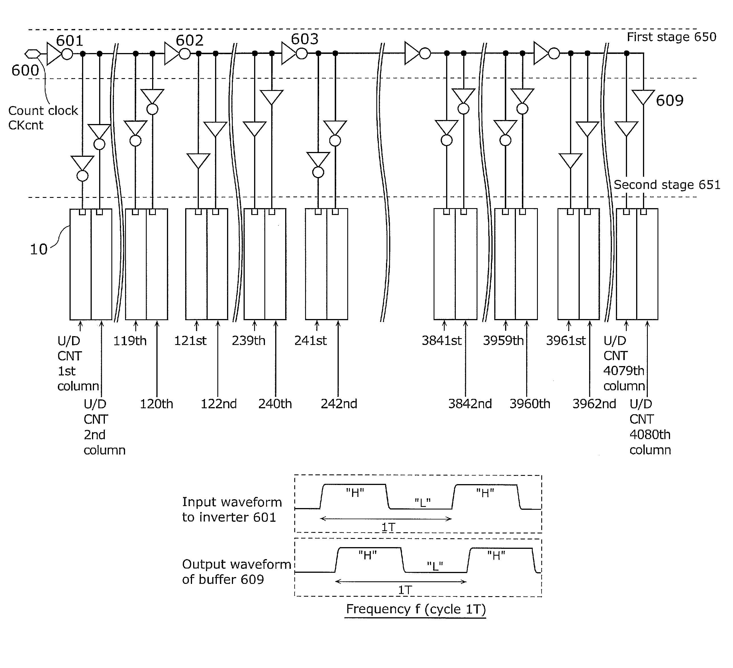
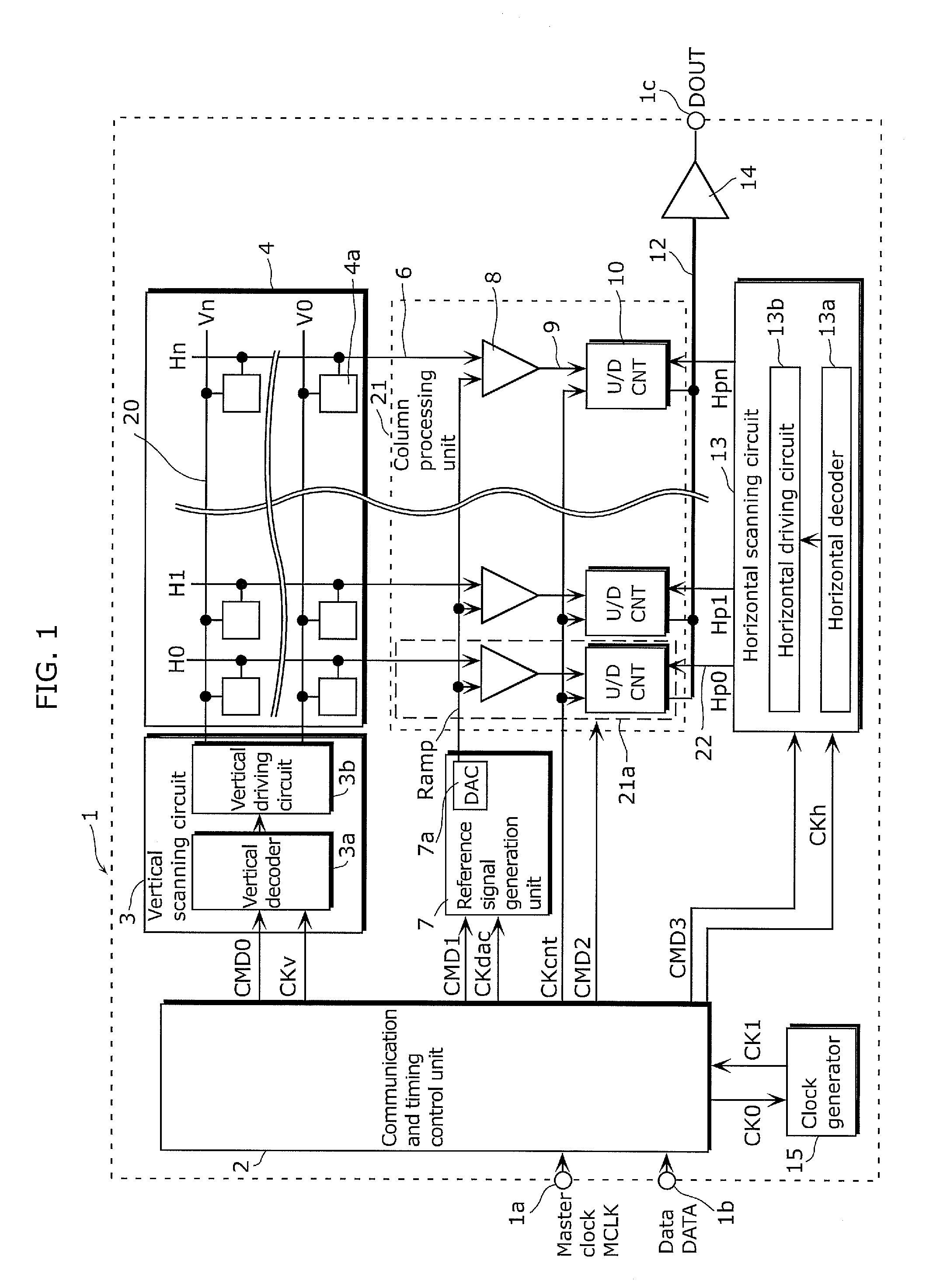
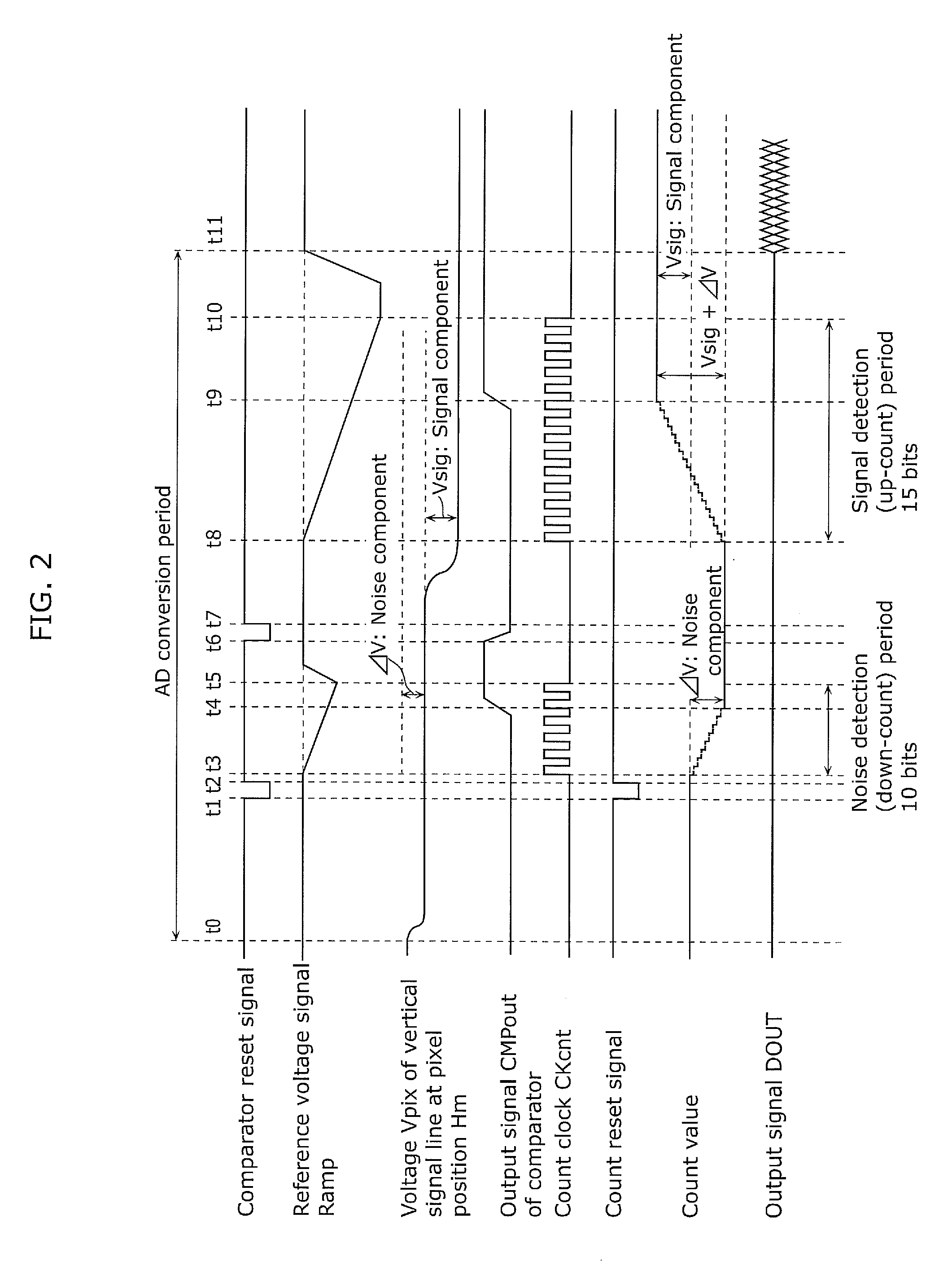
[0063]A solid-state imaging device according to the present embodiment includes a column processing unit which includes: a DA conversion circuit which generates ramp waves; a comparator which compares a pixel signal with a ramp wave signal; and a counter circuit in which a period of time is measured until the pixel signal and the ramp wave signal match and the result is held as a count value. The column processing unit includes a first stage which has first inverters sequentially connected, as a buffering means for operating the counter circuit, and disposed at an equal interval to a farthest end portion of a column, and a second stage in which second inverters having m columns are connected in parallel to an output terminal of the odd-numbered first inverter in the first stage while buffers of m columns are connected in parallel to an output terminal of the even-numbered first inverter. Then, the second inverter and the buffers in the second stage are connected to a counter circuit...

embodiment 2

[0141]Embodiment 2 of the present invention will be described with reference to the drawings. It should be noted that the description will focus on the difference from Embodiment 1 and the remaining part is the same as Embodiment 1.

[0142]FIG. 5 is a block diagram of a clock tree of a count clock for use in the MOS-type solid-state imaging device according to Embodiment 2 of the present invention.

[0143]The count clock CKcnt generated by the communication and timing control unit 2 is inputted into an input terminal 700 and is buffered as needed by inverters (so-called repeaters) regularly (every 120 columns in the present configuration) disposed until the column far end portion (4080th column in FIG. 5). In other words, the column processing unit 21 has a plurality of the first inverters in which all the counter circuits 10 are connected at a substantially equal interval to be along a one dimensionally arranged direction and the number of inverters is less than the number of pixel col...

embodiment 3

[0149]FIG. 6 is a functional block diagram of an imaging device (camera) according to Embodiment 3 of the present invention.

[0150]As illustrated in FIG. 6, an imaging device 30 according to the present invention generally includes an optical system 100, a solid-state imaging device 200, an image processing circuit 300, and a camera system control unit 400.

[0151]The optical system 100 includes a lens 101 which collects light from an object and forms an image on a pixel array of the solid-state imaging device 200 that is the solid-state imaging device which is described in Embodiment 1 and Embodiment 2 of the present invention.

[0152]The solid-state imaging device 200 includes a pixel array 4 in which unit pixels including a light-sensitive element such as a photodiode and a MOS transistor are arranged in a two-dimensional array, a vertical scanning circuit 3 which selects a unit pixel 4a of the pixel array 4 on a row-by-row basis and controls a pixel reset and readout, a column AD cir...


PUM


Abstract

A solid-state imaging device includes: a column comparison circuit which compares a pixel signal with ramp waves and detects a timing at which the pixel signal and the ramp waves match; a counter circuit which is disposed for each of the pixel columns and measures the timing in the column comparison circuit by being supplied with a clock signal; and M first inverters which are equidistantly connected in series, wherein the counter circuit belongs to one of M groups corresponding to each of the M first inverters disposed in the upper clock stage, the odd-numbered group has second inverters disposed between the output terminal of the first inverter corresponding to the group and the counter circuit of the group, and the even-numbered group has buffers disposed between the output terminal of the first inverter corresponding to the group and the counter circuit of the group.

Description

CROSS REFERENCE TO RELATED APPLICATIONS[0001]This is a continuation application of PCT Patent Application No. PCT / JP2010 / 005933 filed on Oct. 4, 2010, designating the United States of America, which is based on and claims priority of Japanese Patent Application No. 2010-042645 filed on Feb. 26, 2010. The entire disclosures of the above-identified applications, including the specifications, drawings and claims are incorporated herein by reference in their entirety.TECHNICAL FIELD[0002]The present invention relates to solid-state imaging devices and imaging devices, and, in particular, to a solid-state imaging device and an imaging device which have an analog-to-digital (AD) conversion function.BACKGROUND ART[0003]A Metal Oxide Semiconductor (MOS) sensor has an analog signal output scheme in which a signal read out from a pixel is outputted as an analog signal, and a digital signal output scheme in which a signal read out from a pixel is outputted as a digital signal by converting an ...

Claims


Application Information

Patent Timeline
Patent Type & Authority Patents(United States)
IPC IPC(8): H04N5/335H03M1/34H01L27/00H04N5/3745H01J40/14H04N5/378
CPCH04N5/378H04N5/37455H04N5/3765H04N5/3577H04N5/374H04N25/617H04N25/745H04N25/76H04N25/75H04N25/772
Inventor SHIMIZU, YUSUKESHIMOMURA, KENICHI
Owner PANASONIC SEMICON SOLUTIONS CO LTD
Why Eureka
Try Eureka