Detector for use in charged-particle microscopy

a technology of charged particles and detectors, applied in instruments, heat measurement, nuclear engineering, etc., can solve the problems of affecting the degree of signal loss, and the necessity of large volume of the pmt tub

Active Publication Date: 2014-05-27
FEI CO
View PDF33 Cites 11 Cited by
  • Summary
  • Abstract
  • Description
  • Claims
  • Application Information

AI Technical Summary

Problems solved by technology

For example, the vitreous tube of the PMT is necessarily quite bulky, seeing as it has to accommodate multiple electrodes in a specific mutual configuration, and has to support high internal vacuum.
Such bulkiness is exacerbated by the fact that each electrode requires an electrical connection through the wall of the vitreous tube to the tube's exterior, where it is connected via an electrical cable to a high-voltage source (typically operating in the kV range).
In addition, a light guide between the scintillator and the PMT may necessarily be quite long (e.g. due to spatial restrictions in placement of the PMT), and this will generally lead to some degree of signal loss.
Moreover, the very principle of operation of the PMT results in a relatively large ultimate electrical current for each electron that strikes the scintillator; consequently, in a scenario in which irradiation of a sample by an imaging beam produces a relatively large flux of output radiation from the sample, this can result in an excessive electrical current at the anode of the PMT.
To mitigate this effect, one can attempt to attenuate the input to the PMT in some way, e.g. by making the employed scintillator less sensitive, but such action will generally tend to complicate the detector set-up even further.

Method used


Image

  • Detector for use in charged-particle microscopy
  • Detector for use in charged-particle microscopy
  • Detector for use in charged-particle microscopy

Examples


embodiment 1

[0033]Multi-Pixel Photon Counters are commercially available from firms such as Hamamatsu Photonics KK, Japan (for example). A Multi-Pixel Photon Counter typically comprises a 2-dimensional array of several hundred or several thousand individual Geiger-APDs, integrated on a small chip. Such a chip typically has lateral dimensions of the order of about 3×3 mm2. In some cases, such chips can be housed in a (metal, ceramic or plastic) canister provided with electrical connection leads; however, such a canister is not necessary, and “naked” Multi-Pixel Photon Counter chips are also commercially available.

[0034]To appreciate the scale of such Multi-Pixel Photon Counter chips, the following comparison is merited. As a reference, an evacuated PMT (photomultiplier tube) with a (typical) diameter of the order of about 2½ cm and a (typical) length of the order of about 10 cm will have a volume of the order of about 80 cm3. In contrast, a canister as referred to above will typically have a vol...

embodiment 2

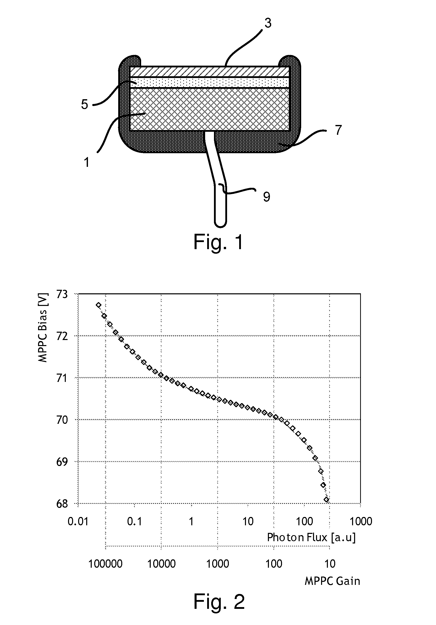
[0046]FIG. 1 shows a cross-sectional view of a particular embodiment of a composite Multi-Pixel Photon Counter-based detector that, in accordance with the present invention, can be used in a charged-particle microscope. The figure shows a (naked) Multi-Pixel Photon Counter chip 1 that is separated from a scintillator 3 via an interposed layer 5 of optically transparent material, such as glass or a suitable type of grease, for instance. The scintillator 3 may comprise a YAG (Yttrium Aluminium Garnet) crystal, for example.

[0047]The interposed (light guide) layer 5 serves to (partially) match the refractive indices of the scintillator 3 and Multi-Pixel Photon Counter 1, and also to electrically isolate them from one another. In use, the Multi-Pixel Photon Counter 1 will be operated at a relatively low voltage, whereas the scintillator 3 will often be maintained at a relatively high electrical potential (typically of the order of kV). To prevent arc-over, the sandwiched assembly 3, 5, 1...

embodiment 3

[0049]FIG. 2 shows a graph of gain versus bias for a particular embodiment of an Multi-Pixel Photon Counter, obtained using the insights underlying the current invention and exploitable according to the invention in a detector for application in a charged-particle microscope. In this specific case, the Multi-Pixel Photon Counter is a type / model S10931-25P, obtainable from Hamamatsu Photonics KK, Japan, and containing a 2-dimensional array of 14400 Geiger-APDs in a 3×3 mm2 die (chip) area. For this particular Multi-Pixel Photon Counter, the manufacturer specified an operating voltage of approximately 74V; however, for other Multi-Pixel Photon Counters, manufacturers can specify different operating voltages (depending inter alia on the details of the integrated circuit design in the MPPC in question).

[0050]In a test associated with the present invention, the Multi-Pixel Photon Counter in question was subjected to an out-of-spec operating voltage. The graph in FIG. 2 shows the surprisi...


PUM


Abstract

A method of investigating a sample using a charged-particle microscope is disclosed. By directing an imaging beam of charged particles at a sample, a resulting flux of output radiation is detected from the sample. At least a portion of the output radiation is examined using a detector, the detector comprising a Solid State Photo-Multiplier. The Solid State Photo-Multiplier is biased so that its gain is matched to the magnitude of output radiation flux.

Description

[0001]This Application claims priority from U.S. Provisional Application 61 / 442,546, filed Feb. 14, 2011, which is hereby incorporated by reference.TECHNICAL FIELD OF THE INVENTION[0002]The invention relates to a method of investigating a sample using a charged-particle microscope.BACKGROUND OF THE INVENTION[0003]Electron microscopy is a well-known technique for imaging microscopic objects. The basic genus of electron microscope has undergone evolution into a number of well-known apparatus species, such as the Transmission Electron Microscope (TEM), Scanning Electron Microscope (SEM), and Scanning Transmission Electron Microscope (STEM), and also into various sub-species, such as so-called “dual-beam” tools (that additionally employ a “machining” beam of ions, allowing supportive activities such as ion-beam milling or ion-beam-induced deposition, for example). In traditional electron microscopes, the imaging beam is “on” for an extended period of time during a given imaging session;...

Claims


Application Information

Patent Timeline
Patent Type & Authority Patents(United States)
IPC IPC(8): H01J37/244
CPCH01J2237/2441H01J37/28H01J2237/31749H01J2237/2445H01J37/244H01J2237/26H01J2237/2605G01N21/6447G01N2201/08H01J37/224H01J37/226H01J2237/2443H01J2237/2802
Inventor HLAVENKA, PETRUNCOVSKY, MAREK
Owner FEI CO
Why Eureka
Try Eureka