
Sensor and method for its production

a technology of sensors and production methods, applied in the field of sensors, can solve the problems of not allowing the development of more complex sensors with high resolution and low nois

Active Publication Date: 2014-06-10
ROBERT BOSCH GMBH
View PDF22 Cites 2 Cited by
  • Summary
  • Abstract
  • Description
  • Claims
  • Application Information

AI Technical Summary

Benefits of technology

This patent describes a MEMS component with a detector region and circuit region that can be formed on one chip. The detector region includes sensor elements, while the circuit region includes additional components to evaluate the sensor elements. The sensor elements are suspended underneath a diaphragm, which is formed by a layer of oxide or dielectric applied on the epitaxy layer and patterned. The diaphragm is self-supporting and accommodates the sensor element in thermally and mechanically decoupled manner. This design allows for excellent thermal decoupling and low signal noise. The use of a diaphragm also enables the routing of individual or groups of sensor elements through the suspension springs. The patent thus describes a high-resolution and low-noise MEMS component suitable for temperature and gas concentration measurements.

Problems solved by technology

However, such production methods often do not allow the development of more complex sensors having high resolution and low noise.

Method used


Image

  • Sensor and method for its production
  • Sensor and method for its production
  • Sensor and method for its production

Examples


Embodiment Construction

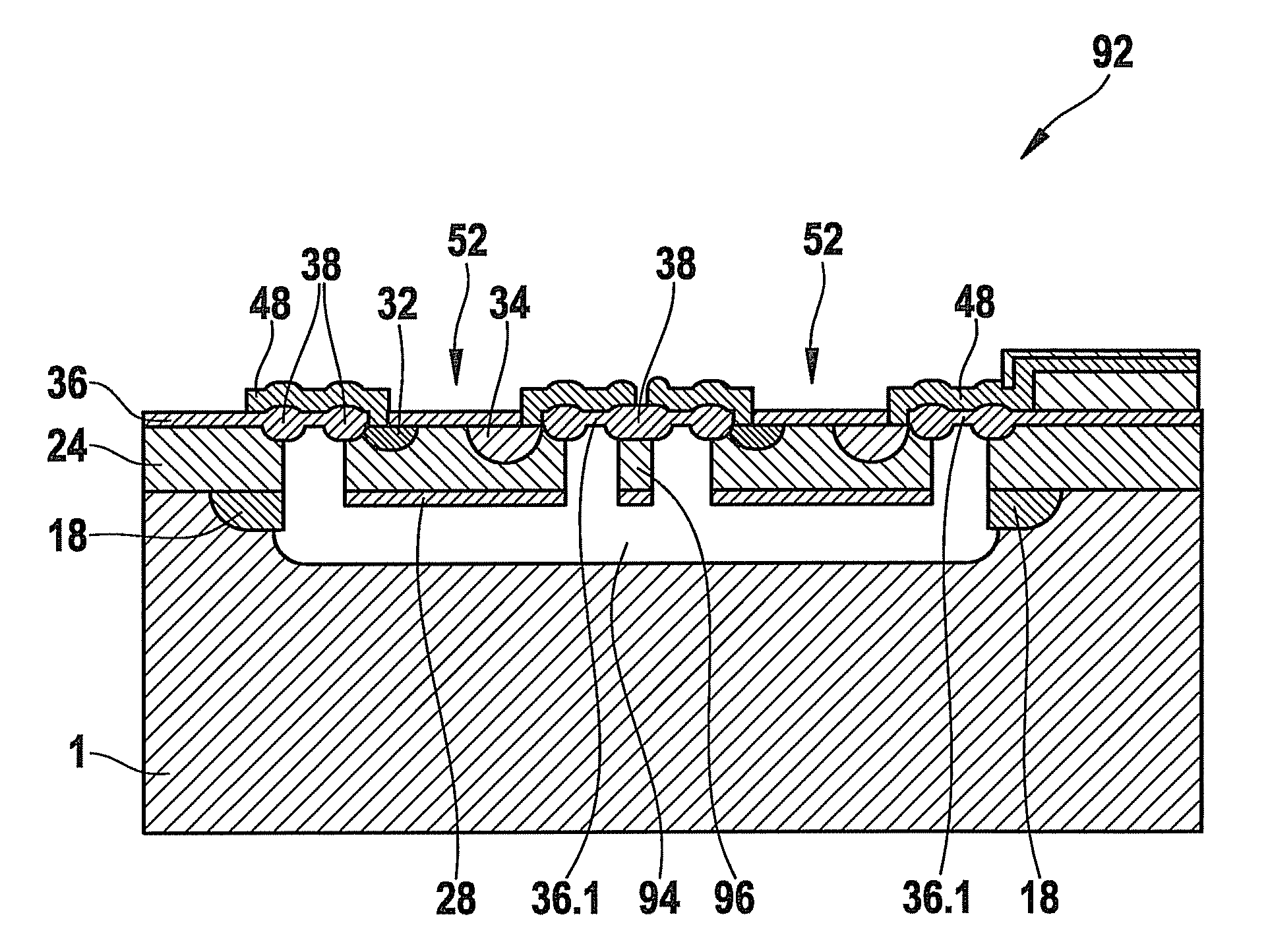
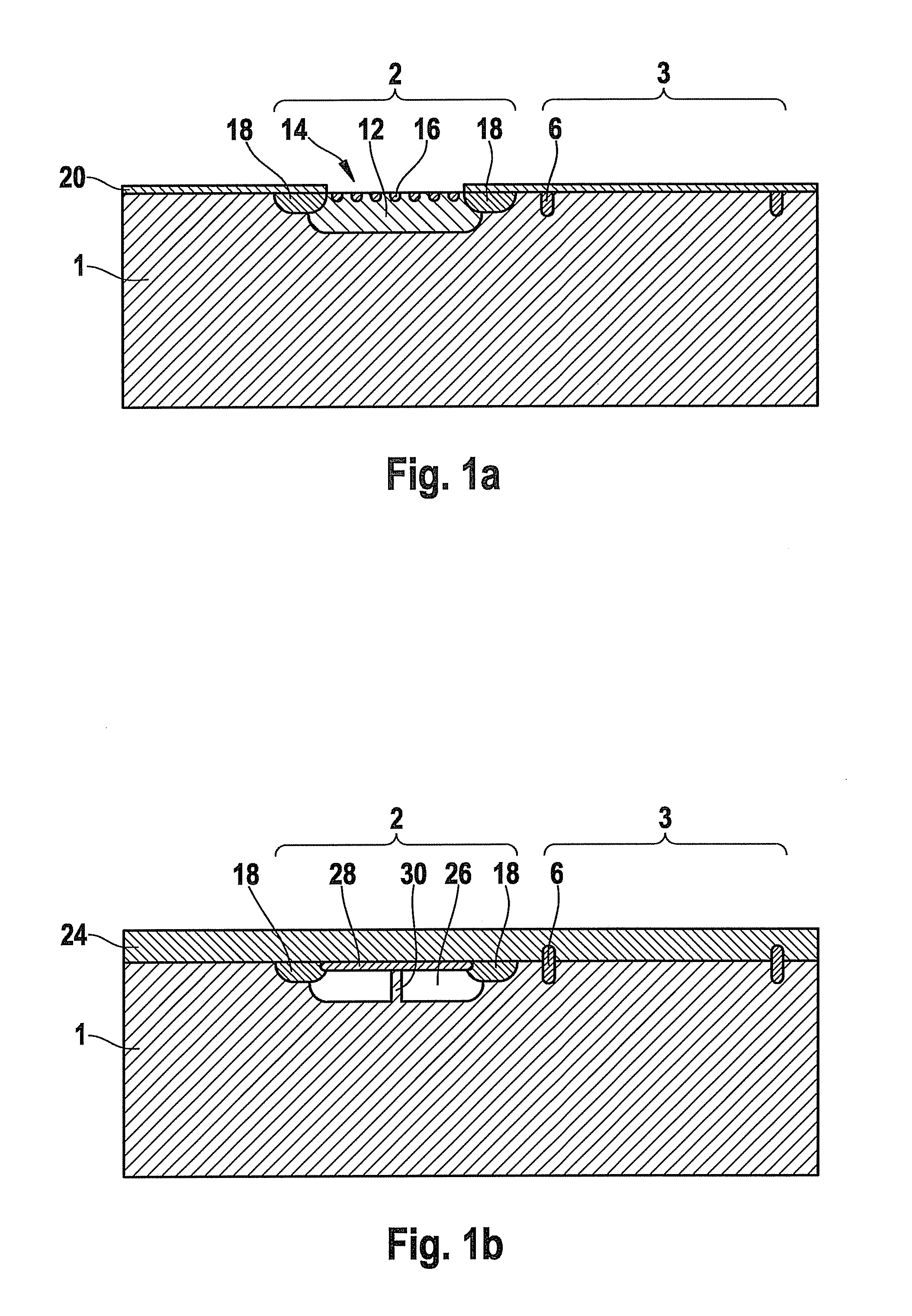
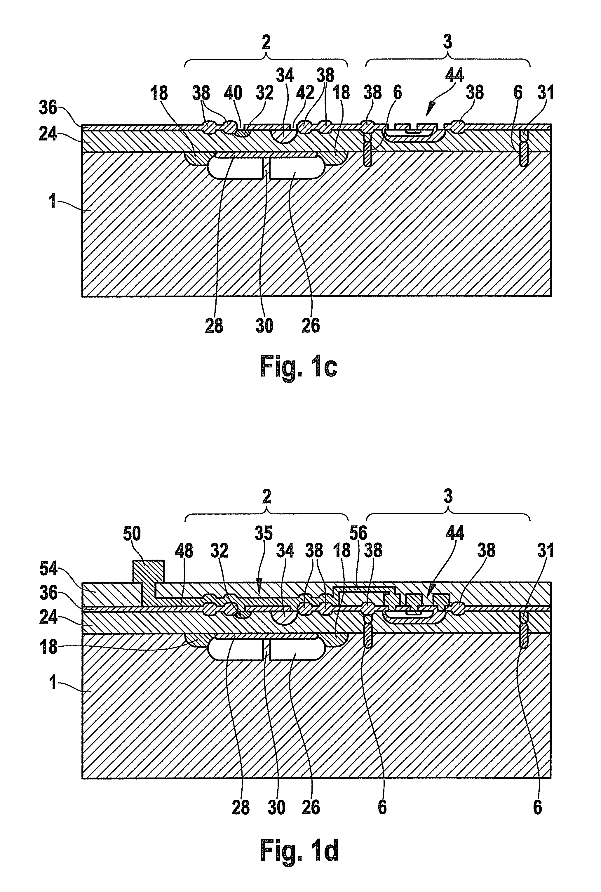
[0029]In the production process, a detector region 2 and, laterally spaced apart or abutting, a circuit region 3 are formed on a p-semiconductor substrate 1, e.g., p-doped (100) silicon; the development of the two regions 2, 3 is able to be fully or partially combined in the subsequent process steps.

[0030]According to FIGS. 1a through 1f, both the circuit region 3 and detector region 2 are implemented in surface-micromechanical manner from the top surface of p-substrate 1. To this end, preliminary circuit processes to form circuit region 3 may be implemented to begin with. Process steps for forming circuit region 3 may also be added between the subsequent process steps 1a through 1f. In an advantageous manner, one or several of the following process steps for developing detector region 3 is / are simultaneously utilized to produce circuit region 3.

[0031]Using p+ doping, for example, a lower iso-layer 6, which has the shape of a trough in cross section, may be formed in p-substrate 1 b...


PUM


Abstract

A sensor, in particular for the spatially resolved detection, includes a substrate, at least one micropatterned sensor element having an electric characteristic whose value varies as a function of the temperature, and at least one diaphragm above a cavity, the sensor element being disposed on the underside of the at least one diaphragm, and the sensor element being contacted via connecting lines, which extend within, on top of or underneath the diaphragm. In particular, a plurality of sensor elements may be formed as diode pixels within a monocrystalline layer formed by epitaxy. Suspension springs, which accommodate the individual sensor elements in elastic and insulating fashion, may be formed within the diaphragm.

Description

FIELD OF THE INVENTION[0001]The present invention relates to a sensor, in particular for the spatially resolved detection, and to a method for its production.BACKGROUND INFORMATION[0002]DE 101 14 036 describes a method for producing micropatterned sensors, in which openings are introduced into a semiconductor substrate, which transform themselves into cavities underneath a sealed diaphragm cover in the depth of the substrate in a subsequent thermal treatment. This makes it possible to produce a capacitive pressure sensor, the cavity in the substrate being developed between two doping zones, which form a plate-type capacitor having a capacitance as a function of the spacing of the doping zones. The doping zones are connected to a corresponding evaluation circuit by deep contacting.[0003]DE 10 2004 043 357 describes a method for producing a cavity in a semiconductor substrate, in which a lattice-type structure on the surface of the substrate is first produced from substrate material n...

Claims


Application Information

Patent Timeline
Patent Type & Authority Patents(United States)
CPCG01J5/20B81B3/0081G01J5/06B81B2203/0109B81B2201/0278B81B2207/015B81C2201/0109
Inventor BENZEL, HUBERTARMBRUSTER, SIMONHOECHST, ARNIMSCHELLING, CHRISTOPHFEYH, ANDO
Owner ROBERT BOSCH GMBH
Learn More