Optical information recording medium and method of recording and/or reproducing therein
a technology of optical information and recording medium, which is applied in the direction of instruments, photomechanical equipment, and thermography, etc., can solve the problems of difficult preparation of organic dyes, difficult to achieve the construction of recording medium layers through the conventional simple process, and different conditions, so as to ensure the cost of recording medium manufacture and the margin of manufacturing process , the effect of stable preservation
- Summary
- Abstract
- Description
- Claims
- Application Information
AI Technical Summary
Benefits of technology
Problems solved by technology
Method used
Image
Examples
example 1
[0063]The optical information recording medium 1 on which recording / reading is performed by an optical disk recording / reading apparatus that employs two groups of objective lenses having a numerical aperture of 0.85 and a semiconductor laser light source which emits light at a wavelength of 405 nm within the wavelength band of blue violet was fabricated as mentioned below.
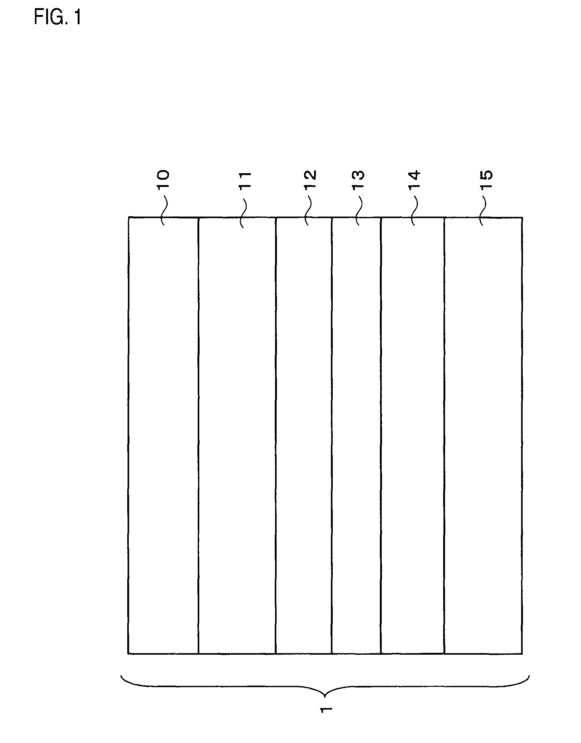
[0064]As the substrate 10, a polycarbonate substrate having grooves, which had a thickness of 1.1 mm, a track pitch of 0.32 μm, and a groove depth of 20 nm, in one side thereof was fabricated using an injection mold. On the polycarbonate substrate, an Ag alloy film of 100 nm thick serving as the reflective layer 11, a Ta2O5 film of 30 nm thick serving as the protective layer 12, the recording layer 13 of 20 nm thick, and a Ta2O5 film of 30 nm thick serving as the protective layer 14 were sequentially formed according to a sputtering method. Further, after an ultraviolet curable type adhesive was applied to the uppe...
example 2
[0093]The optical information recording medium 4 on which recording / reading is performed by an optical disk recording / reading apparatus employing two groups of objective lenses that have a numerical aperture of 0.85 and a semiconductor laser light source that emits light at a wavelength of 405 nm within the wavelength band of blue violet was fabricated as mentioned below.
[0094]As the substrate 10, a polycarbonate substrate having grooves, which had a thickness of 1.1 mm, a track pitch of 0.32 μm, and a groove depth of 20 nm, on one side thereof was fabricated using an injection mold. On the polycarbonate substrate, an Ag alloy film of 100 nm thick serving as the reflective layer 11, a Ta2O5 film of 30 nm thick serving as the protective layer 12, the recording layer 13 of 20 nm thick, and a Ta2O5 film of 30 nm thick serving as the protective layer 14 were sequentially formed according to the sputtering method. After an adhesive of an ultraviolet curable type was applied to the Ta2O5 ...
PUM
| Property | Measurement | Unit |
|---|---|---|
| thickness | aaaaa | aaaaa |
| thickness | aaaaa | aaaaa |
| wavelength | aaaaa | aaaaa |
Abstract
Description
Claims
Application Information


