
Electron beam plasma chamber

a plasma chamber and electron beam technology, applied in plasma technology, solid-state diffusion coatings, coatings, etc., can solve the problems of reducing affecting the efficiency of plasma processing, and affecting the quality of plasma processing, so as to improve the deposition process and deposited film properties, increase the temperature of the substrate, and improve the effect of electrical quality

Inactive Publication Date: 2014-07-01
APPLIED MATERIALS INC
View PDF9 Cites 2 Cited by
  • Summary
  • Abstract
  • Description
  • Claims
  • Application Information

AI Technical Summary

Benefits of technology

This patent describes methods for using electron beams to improve the deposition process and obtain better film properties. The energy of the electron beams can be adjusted to increase the formation of desired species, such as ions or radicals, which aid in the deposition process. In one embodiment, ions are maximized for high aspect fill by applying a high electron beam energy, while in another embodiment, radicals are maximized for depositing an oxide with good electrical quality by applying a low electron beam energy. The patent also describes an electron beam chamber wherein electron beams are directed as a sheet perpendicular to a gas stream flowing towards a substrate, which can be scanned across a large area of a moving substrate to increase throughput. The distance between the electron beams and the substrate and the temperature of the substrate can be controlled for better conformality.

Problems solved by technology

Too many radicals may grow on the sidewall and top corner of the trench and result in pinch-off of the feature.
Additionally, delivery of the different types of active species can only be tuned by making major hardware changes in the processing chamber such as adding an ion filter, a remote plasma, or changing the showerhead.
However, true separation of ion and radical species can generally not be accomplished using these conventional plasma processing methods.

Method used


Image

  • Electron beam plasma chamber
  • Electron beam plasma chamber
  • Electron beam plasma chamber

Examples


Embodiment Construction

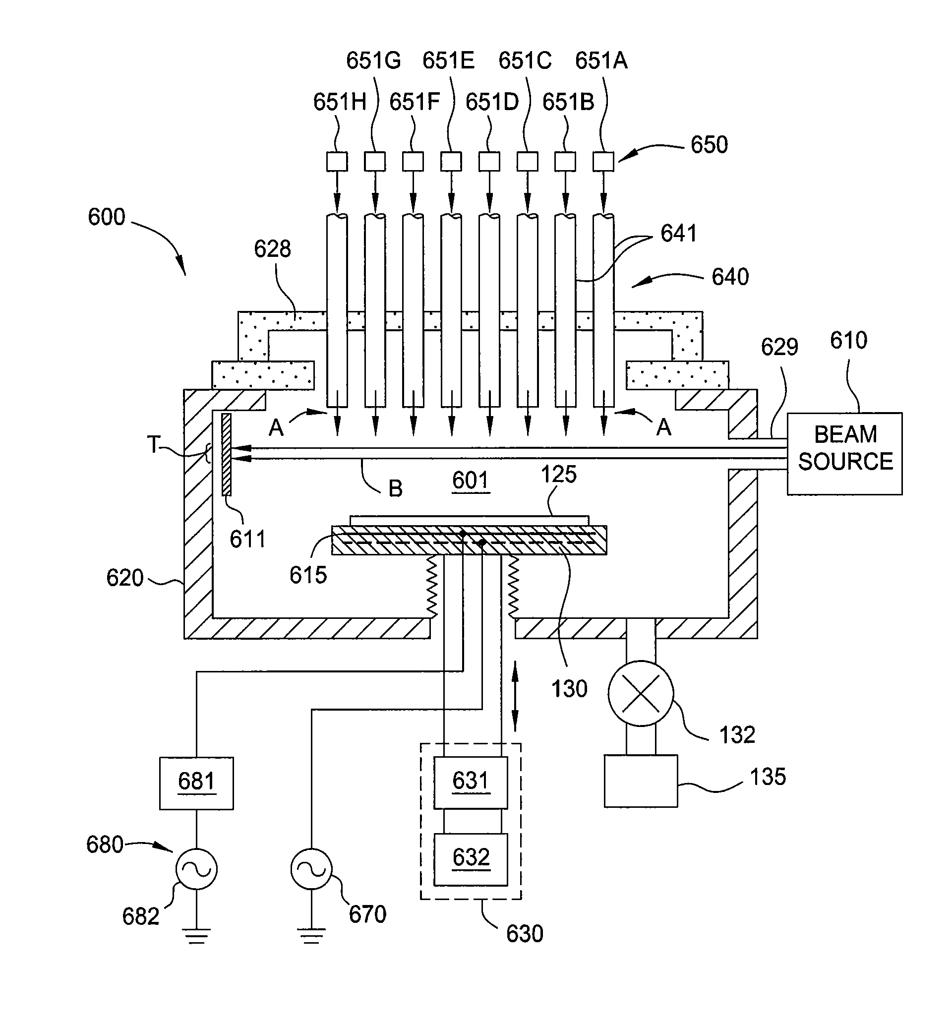
[0023]Embodiments disclosed herein generally relate to a method and apparatus for tailoring the formation of active species using one or more electron beams to improve gap-fill during an integrated circuit formation process. The methods described herein allow the amount of each type of active species to be controlled independently of the other typical process variables, such as process pressure, gas composition. The method described herein tailors the energy of the electron beams to maximize the desired species (e.g., ions or radicals). In one embodiment, the percentage of ions in the processing region of a processing chamber is maximized for high aspect fill by delivering a high electron beam energy to a portion of the processing chamber gas. In another embodiment, the percentage of radicals in the processing region of a processing chamber is maximized by delivering a desirable electron beam energy. In this case, an oxide having good electrical quality can be formed by increasing t...


PUM

PropertyMeasurementUnit
angleaaaaaaaaaa
angleaaaaaaaaaa
sizeaaaaaaaaaa

Abstract

A method and apparatus for tailoring the formation of active species using one or more electron beams to improve gap-fill during an integrated circuit formation process is disclosed herein. The energy of the electron beams may be decreased to maximize electrons leading to radicals or increased to maximize electrons leading to ions, depending on the fill application. An apparatus comprising multiple impinging jets of gas perpendicular to one or more electron beams is also disclosed.

Description

CROSS-REFERENCE TO RELATED APPLICATIONS[0001]This application claims benefit of U.S. Provisional Patent Application Ser. No. 61 / 513,498, filed Jul. 29, 2011, which is herein incorporated by reference.BACKGROUND OF THE INVENTION[0002]1. Field of the Invention[0003]Embodiments of the present invention generally relate to a process and processing chamber that are useful for improving gap-fill during an integrated circuit processing sequence.[0004]2. Description of the Related Art[0005]As semiconductor device geometries continue to decrease in size, providing more devices per unit area on a fabricated substrate has become increasingly important. These devices are initially isolated from each other as they are formed on the substrate, and they are subsequently interconnected to create the specific circuit configurations desired. For example, spacing between devices such as conductive lines or traces on a patterned substrate may be separated by 0.18 μm, leaving recesses or gaps of a compa...

Claims


Application Information

Patent Timeline
Patent Type & Authority Patents(United States)
IPC IPC(8): C23C8/00H05H1/24
CPCH01L21/3065C23C16/487
Inventor ROGERS, MATTHEW, S.
Owner APPLIED MATERIALS INC
Learn More