Gate stack metrology

a technology of gate stack and metrology, applied in the field of integrated circuit fabrication, can solve the problems of increasing the length of data acquisition time needed, limited metal throughput for high-k applications, signal-to-noise ratio, etc., and achieves the effect of fast and simple method of determination, more surface sensitivity, and more sensitive to film stack

Active Publication Date: 2014-07-08
KLA TENCOR TECH CORP
View PDF4 Cites 10 Cited by
  • Summary
  • Abstract
  • Description
  • Claims
  • Application Information

AI Technical Summary

Benefits of technology

[0051]A high brightness ultraviolet source 102 enables the system 100 to acquire valence band spectra (using UPS) in just a few seconds as compared to the tens or hundreds of seconds required by core-level spectra (XPS). The UPS 102 has more surface sensitivity due to a combination of the small penetration depth of the ultraviolet source 102 and the low energy photoelectron small inelastic mean free path. Therefore, UPS is more sensitive to the film stack and provides a fast and simple method to determine the composition of a high-k film stack, without the photoele...

Problems solved by technology

Unfortunately, the data acquisition time that is needed to achieve an acceptable signal-to-noise ratio for either of these two high energy resolution methods is an order of magnitude greater than that which is required by a low energy resolution method (where ΔE=about 1 to 2 eV).
The metrology throughput for high-k applications is ultimately limited by the total data acquisition time for all of the elements that are present.
This further increases the length of the data acquisiti...

Method used


Image

  • Gate stack metrology
  • Gate stack metrology
  • Gate stack metrology

Examples


Embodiment Construction

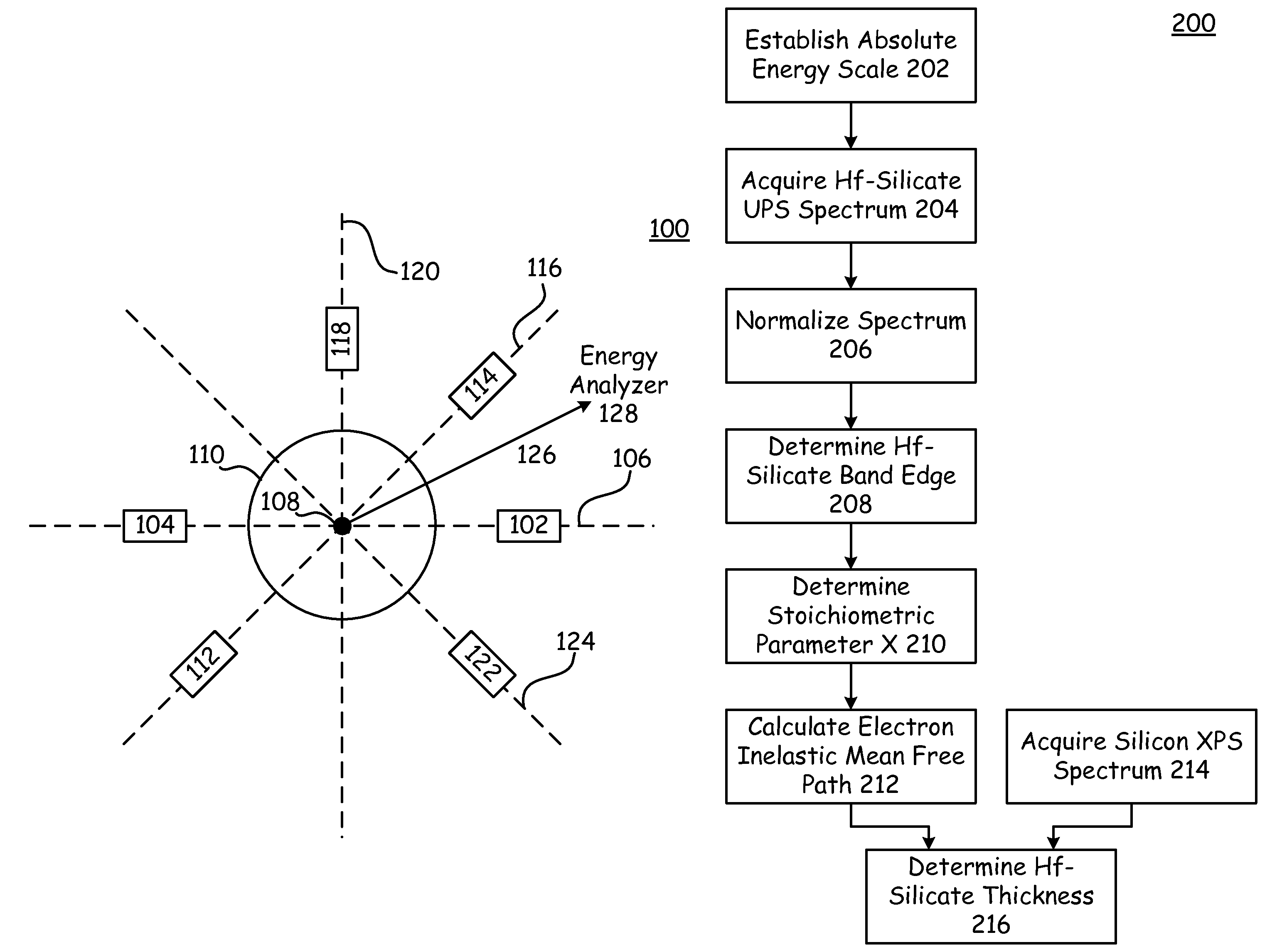
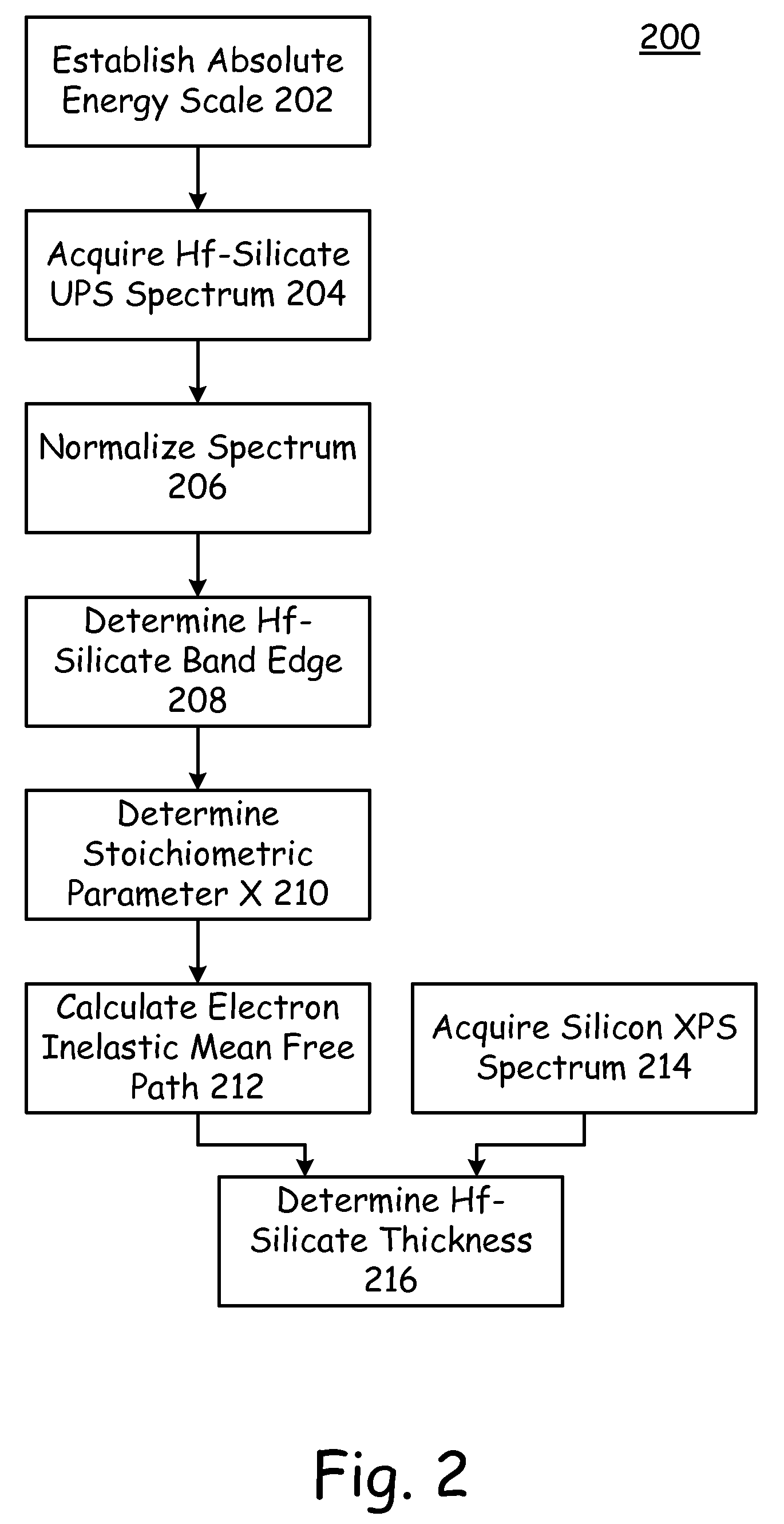
[0026]Various embodiments of the present invention take advantage of the dependence of the band gap of high-k dielectric materials on composition. For example, the band gap of hafnium silicate, (HfO2)x(SiO2)1-x, increases from about 5.5 eV to about 6.6 eV as x decreases from about 0.75 to about 0.25. The valence band is also sensitive to defects in the film. The composition and defects of a gate dielectric film can be determined by measuring the valence band edge shift and the valence state distribution with ultraviolet photoemission spectroscopy. By combining UPS data with XPS data, the thickness and composition measurement results are improved as compared with measurements made individually by XPS or UPS.

[0027]Some embodiments of the invention use an optical measurement such as ellipsometry or reflectometry to determine information about a film layer, such as its direct band gap (Eg), and combine that information with XPS data. The thickness and composition measurement results fro...


PUM


Abstract

An x-ray photoelectron spectroscopy apparatus for measuring film stack characteristics, of the type having an x-ray source and an x-ray photoelectron spectroscopy module coupled to a contiguous vacuum environment, including an ultraviolet source and an ultraviolet photoelectron spectroscopy module coupled to the vacuum environment.

Description

FIELD[0001]This application claims all rights and priority on prior U.S. provisional patent application Ser. No. 61 / 369,650 filed 2010 Jul. 30. This invention relates to the field of integrated circuit fabrication. More particularly, this invention relates to measuring and monitoring physical parameters of gate and capacitor dielectric stacks for process control at high throughput and high precision.INTRODUCTION[0002]X-ray photoelectron spectroscopy (XPS) is used to measure the thickness and composition of thin film stacks. This method involves directing x-ray radiation towards the surface of a sample, thereby causing photoelectrons to be emitted from the surface. The kinetic energy of the photoelectrons that are emitted from the surface is related to the both the properties of the x-ray radiation itself, and the properties of the material from which the surface is comprised, as given by the photoelectron equation:hν=Eb(I)+Ek(I),[0003]where Eb(I) is the binding energy or ionization ...

Claims


Application Information

Patent Timeline
IPC IPC(8): G01N23/20
CPCG01N2223/615G01N2223/611G01N23/2273
Inventor ZHUANG, GHUORONG V.FIELDEN, JOHN
Owner KLA TENCOR TECH CORP
Why Eureka
Try Eureka