Sapphire substrate and nitride semiconductor light emitting device

a technology of semiconductor light emitting device and semiconductor substrate, which is applied in the direction of polycrystalline material growth, crystal growth process, chemically reactive gas, etc., can solve the problems of crystal defects, recent arisen, and not necessarily satisfactory crystallinity of nitride semiconductor grown on a surface with truncated triangular pyramid-shaped dimples, etc., to achieve improved or excellent crystallinity

Active Publication Date: 2014-07-15
NICHIA CORP
View PDF5 Cites 12 Cited by
  • Summary
  • Abstract
  • Description
  • Claims
  • Application Information

AI Technical Summary

Benefits of technology

[0008]Thus, an object of the present invention is to provide a sapphire substrate for a nitride semiconductor light emitting device that enables the growth of a nitride semiconductor having more improved, possibly excellent crystallinity, and also can constitute a nitride semiconductor light emitting device having more improved, even excellent light extraction efficiency, and a method for manufacturing the same.
[0009]Another object of the present invention is to provide a nitride semiconductor light emitting device that includes a nitride semiconductor having excellent crystallinity, and is also excellent in light extraction efficiency.
[0020]In the sapphire substrate according to the present invention constituted as mentioned above, because each of a plurality of projections formed on one principal surface has a pyramidal shape with a substantially sharpened tip, and each inclined surface of the projection is composed of a crystal growth-suppression surface that lessens or suppresses the growth of the nitride semiconductor in comparison with a substrate surface located between adjacent projections, and also has an inclination change line at which an inclination angle discontinuously varies, the sapphire substrate enables the growth of a nitride semiconductor having improved or excellent crystallinity, and also can constitute a nitride semiconductor light emitting device having improved or excellent light extraction efficiency.

Problems solved by technology

However, the present inventors have intensively studied and found that crystallinity of a nitride semiconductor grown on a surface with truncated triangular pyramid-shaped dimples is not necessarily satisfactory.
With the increase of the output of a light emitting diode, problems due to crystal defects, which have not arisen in prior light emitting diodes, have recently arisen.

Method used


Image

  • Sapphire substrate and nitride semiconductor light emitting device
  • Sapphire substrate and nitride semiconductor light emitting device
  • Sapphire substrate and nitride semiconductor light emitting device

Examples


example 1

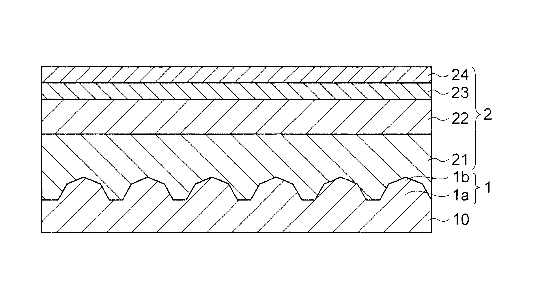
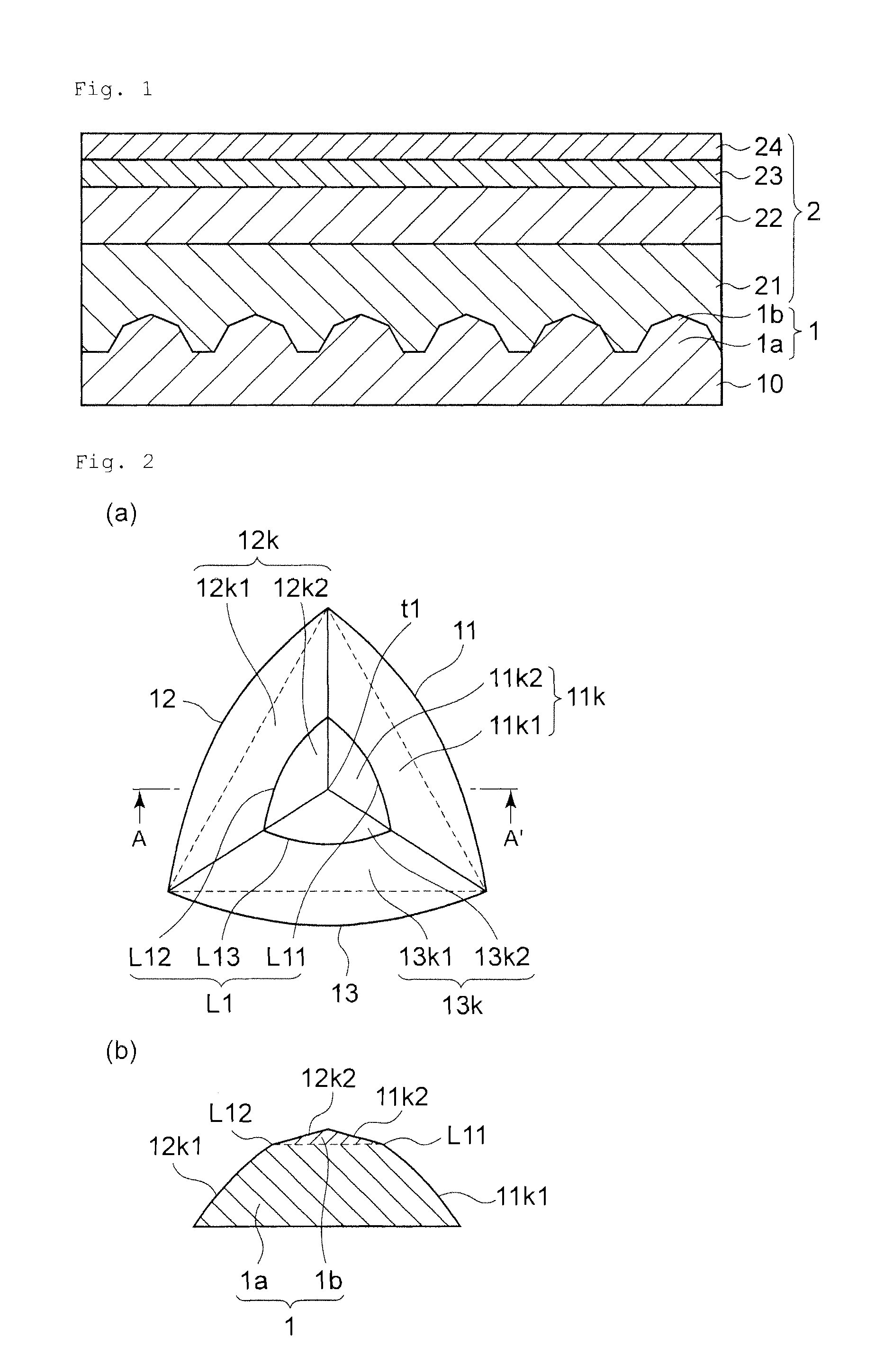
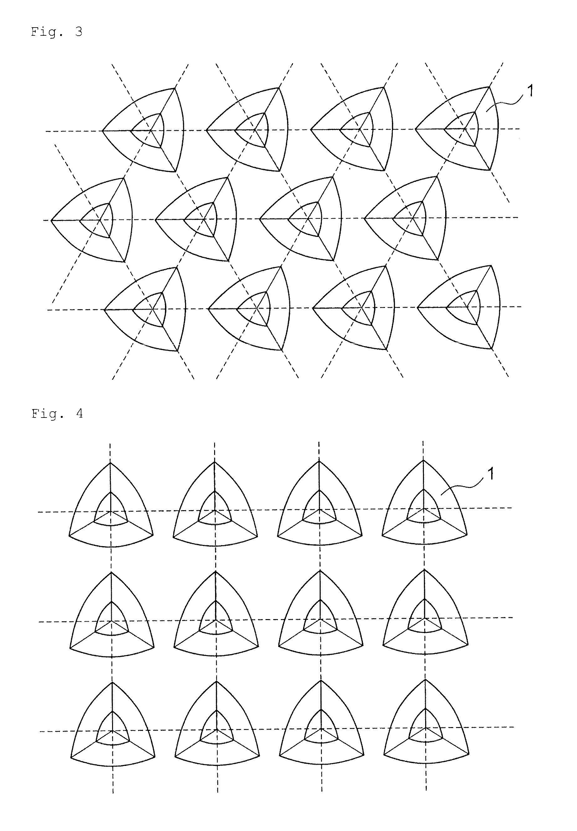
[0070]On the C-plane (0001) of a sapphire substrate, a SiO2 film was formed, followed by patterning to periodically form a circular first mask 19 having a diameter of about 1.5 μm.

[0071]Subsequently, the substrate was immersed in an etching bath using a mixed acid of phosphoric acid and sulfuric acid as an etching solution and etched at a solution temperature of about 290° C. for about 5 minutes until the depth (projection height) becomes about 1 μm.

[0072]Whereby, a lower projection 1a was formed.

[0073]Next, after removing the first mask 19, the substrate was immersed in an etching bath using a mixed acid of phosphoric acid and sulfuric acid as an etching solution, in a state of absence of a mask, and etched at a solution temperature of about 290° for about 1 minute until a tip of projection is substantially sharpened to form an upper projection 1b.

[0074]A projection 1 having a height of about 1 μm and a two-stage taper angle was formed by the aforementioned steps.

[0075]Subsequentl...


PUM

PropertyMeasurementUnit
heightaaaaaaaaaa
heightaaaaaaaaaa
heightaaaaaaaaaa

Abstract

A sapphire substrate having one principal surface on which a nitride semiconductor is grown, said one principal surface having a plurality of projections. Each of the projections has a generally pyramidal shape with a not truncated, more sharpened tip and with an inclined surface composed of a crystal growth-suppression surface that lessens or suppresses the growth of the nitride semiconductor and also which has an inclination change line at which an inclination angle discontinuously varies.

Description

BACKGROUND OF THE INVENTION[0001]1. Field of the Invention[0002]The present invention relates to a sapphire substrate for a nitride semiconductor light emitting device and a method for manufacturing the same, and a nitride semiconductor light emitting device incorporating the sapphire substrate.[0003]2. Description of the Related Art[0004]A light emitting diode (LED) made of a nitride semiconductor is usually constituted by sequentially laminating an n-type semiconductor layer, an active layer and a p-type semiconductor layer on a sapphire substrate. In this light emitting diode, emitted light is extracted from the side opposite the sapphire substrate or the side of the sapphire substrate, while light emitted from the active layer is also radiated in a direction opposite the light emission side. Therefore, it becomes necessary to improve external quantum efficiency by enabling light radiated in a direction opposite the light emission side to be extracted effectively from the light e...

Claims


Application Information

Patent Timeline
Patent Type & Authority Patents(United States)
IPC IPC(8): H01L33/00
CPCC30B25/183H01L33/12C30B25/186H01L21/0254C30B29/403H01L33/32H01L21/02658H01L21/0242H01L21/0243
Inventor NARITA, JUNYAWAKAI, YOHEIWAKAKI, TAKAYOSHI
Owner NICHIA CORP
Why Eureka
Try Eureka