Glass substrate for a magnetic disk and magnetic disk

a technology of magnetic disk and glass substrate, which is applied in the field of glass substrate for a magnetic disk and a magnetic disk, can solve the problems of stamper damage, etc., and achieve the effects of easy removal of foreign matter, high recording density, and increased chemical affinity

Active Publication Date: 2014-07-22
HOYA CORP
View PDF27 Cites 8 Cited by
  • Summary
  • Abstract
  • Description
  • Claims
  • Application Information

AI Technical Summary

Benefits of technology

[0022]In the magnetic disk glass substrate of this invention, an arithmetic mean roughness (Ra) of a main surface of the glass substrate measured using an atomic force microscope with a resolution of 256×256 pixels in a 2 μm×2 μm square is 0.12 nm or less and, among defects detected to have a size of 0.1 μm or more and 0.3 μm or less upon irradiating light with a wavelength of 405 nm onto the glass substrate with a spot size of 5 μm and detecting scattered light from the glass substrate, the number of the defects fixed to the glass substrate is 1 or less per 24 cm2. Accordingly, the number of defects present on the surface with the arithmetic mean roughness (Ra) at the level in the vicinity of 0.1 nm is very small.
[0023]Therefore, it is suitable as a substrate for manufacturing a magnetic disk having magnetic particles with a much smaller size, for example, having a recording density of 160 GB or more per disk, particularly 250 GB or more per disk.
[0024]In the magnetic disk glass substrate of this invention, an arithmetic mean roughness (Ra) of a main surface of the glass substrate measured using an atomic force microscope with a resolution of 256×256 pixels in a 2 μm×2 μm square is 0.12 nm or less and the number of defects detected to have a size of 0.1 μm or more and 0.6 μm or less in plan view and a depth of 0.5 nm or more and 2 nm or less is less than 10 per 24 cm2, the defects each being detected using a shift in wavelength between incident light and reflected light upon irradiating and scanning helium neon laser light with a wavelength of 632 nm on the main surface of the glass substrate. Accordingly, the number of defects present on the surface with the arithmetic mean roughness (Ra) at the level in the vicinity of 0.1 nm is very small.
[0025]Therefore, it is suitable as a substrate for manufacturing a magnetic disk having magnetic particles with a much smaller size, for example, having a recording density of 160 GB or more per disk, particularly 250 GB or more per disk.
[0026]Further, according to the magnetic disk glass substrate manufacturing method of this invention, since the additive contained in the polishing liquid used in the polishing step is contained in the cleaning liquid, it is possible, in the cleaning step, to remove foreign matter (adhering matter) from the surface of the glass substrate while maintaining the form of secondary aggregation of the polishing agent and maintaining the interaction thereof with the surface of the glass substrate. Further, with the above-mentioned configuration, it is possible to easily remove the foreign matter by increasing the chemical affinity. As a consequence, it is possible to manufacture a magnetic disk glass substrate which has very few defects present on its surface with an arithmetic mean roughness (Ra) at a level in the vicinity of 0.1 nm and thus is suitable as a substrate for a magnetic disk with high recording density.

Problems solved by technology

Further, depending on circumstances, there is a possibility of damage to the stamper.

Method used


Image

  • Glass substrate for a magnetic disk and magnetic disk
  • Glass substrate for a magnetic disk and magnetic disk
  • Glass substrate for a magnetic disk and magnetic disk

Examples


embodiment 1

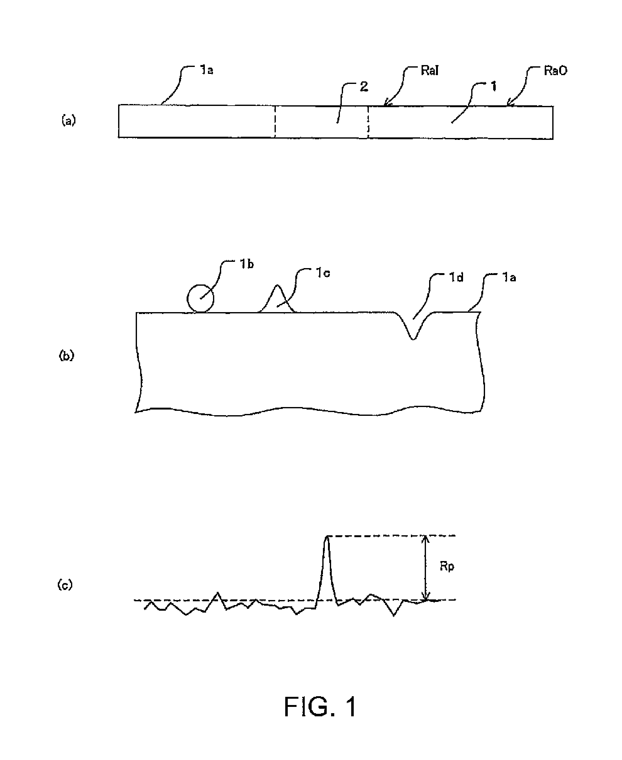
[0035]FIG. 1 shows diagrams of a magnetic disk glass substrate according to an embodiment 1, wherein (a) is a side view, (b) is a diagram for explaining defects present on a surface thereof, and (c) is a diagram for explaining the roughness of the surface.

[0036]A magnetic disk glass substrate 1 shown in FIG. 1 is such that an arithmetic mean roughness (Ra) of a main surface of the glass substrate measured using an atomic force microscope with a resolution of 256×256 pixels in a 2 μm×2 μm square is 0.12 nm or less and, among defects detected to have a size of 0.1 μm or more and 0.3 μm or less upon irradiating light with a wavelength of 405 nm onto the glass substrate with a spot size of 5 μm and detecting scattered light from the glass substrate, the number of the defects fixed to the glass substrate is 1 or less per 24 cm2.

[0037]As shown in FIG. 1(b), defects present on a surface 1a of the magnetic disk glass substrate 1 include adhering matter 1b of the kind that can be easily remo...

embodiment 2

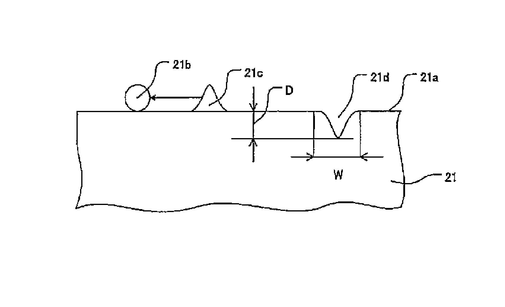
[0057]FIG. 3 is a diagram for explaining defects present on a surface of a magnetic disk glass substrate according to an embodiment 2.

[0058]A magnetic disk glass substrate 21 shown in FIG. 3 is such that an arithmetic mean roughness (Ra) of a main surface of the glass substrate measured using an atomic force microscope with a resolution of 256×256 pixels in a 2 μm×2 μm square is 0.12 nm or less and the number of defects detected to have a size of 0.1 μm or more and 0.6 μm or less in plan view and a depth of 0.5 nm or more and 2 nm or less is less than 10 per 24 cm2, the defects each being detected using a shift in wavelength between incident light and reflected light upon irradiating and scanning helium neon laser light with a wavelength of 632 nm on the main surface of the glass substrate.

[0059]As shown in FIG. 3, defects present on a surface 21a of the magnetic disk glass substrate 21 include adhering matter 21b of the kind that can be easily removed by cleaning, and a convex defe...

embodiment 3

[0070]In this embodiment, a magnetic disk glass substrate manufacturing method will be described.

[0071]The magnetic disk glass substrate manufacturing method according to this embodiment comprises a process of applying at least shaping and lapping to a glass substrate having a pair of main surfaces, a polishing process of polishing the main surfaces, and a cleaning process of cleaning the glass substrate after the polishing, wherein an additive contained in a polishing liquid for use in the polishing process is contained in a cleaning liquid for use in the cleaning process.

[0072]More specifically, the manufacture of a magnetic disk glass substrate comprises (1) Shaping Process and First Lapping Process, (2) End Portion Shaping Process (coring process for forming a hole and chamfering process for forming chamfered faces at end portions (outer peripheral end portion and inner peripheral end portion) (chamfered face forming process)), (3) End Face Polishing Process (outer peripheral en...


PUM

PropertyMeasurementUnit
sizeaaaaaaaaaa
sizeaaaaaaaaaa
sizeaaaaaaaaaa

Abstract

Provided are a magnetic disk substrate and a method of manufacturing the same, wherein the magnetic disk substrate has very few defects present on its surface with an arithmetic mean roughness (Ra) at a level in the vicinity of 0.1 nm and thus is suitable as a substrate for a magnetic disk with high recording density. The magnetic disk glass substrate is such that the arithmetic mean roughness (Ra) of the main surface of the glass substrate measured using an atomic force microscope with a resolution of 256×256 pixels in a 2 μm×2 μm square is 0.12 nm or less and the number of defects detected to have a size of 0.1 μm to 0.6 μm in plan view and a depth of 0.5 nm to 2 nm is less than 10 per 24 cm2, wherein the defects are each detected using a shift in wavelength between incident light and reflected light upon irradiating and scanning helium neon laser light with a wavelength of 632 nm on the main surface of the glass substrate.

Description

CROSS REFERENCE TO RELATED APPLICATIONS[0001]This application is a National Stage of International Application No. PCT / JP2009 / 066956, filed on Sep. 29, 2009, which claims priority from Japanese Patent Application Nos. 2008-254065 and 2008-254787, filed on Sep. 30, 2008, the contents of all of which are incorporated herein by reference in their entirety.TECHNICAL FIELD[0002]This invention relates to a glass substrate for a magnetic disk adapted to be mounted in a hard disk drive device, and to the magnetic disk.BACKGROUND ART[0003]As a magnetic recording medium adapted to be mounted in a hard disk drive device (HDD device), there is a magnetic disk. The magnetic disk is produced by coating a NiP film on a metal substrate made of an aluminum-magnesium alloy or the like or by laminating a magnetic layer and a protective layer on a glass substrate or a ceramic substrate. Aluminum alloy substrates have conventionally been widely used as substrates for magnetic disks. However, following t...

Claims


Application Information

Patent Timeline
Patent Type & Authority Patents(United States)
IPC IPC(8): C03C23/00B24B7/00G11B5/84B32B3/26C03C21/00
CPCC03C21/008C03C23/0075C09G1/02G11B5/7315C03C2204/08C03C19/00G11B5/8408C03C23/009G11B5/8404G11B5/73921
Inventor EDA, SHINJIISONO, HIDEKIMAEDA, TAKASHITSUCHIYA, HIROSHIMARUMO, YOSHINORI
Owner HOYA CORP
Why Eureka
Try Eureka