Semiconductor device and method for manufacturing the same

a technology of semiconductors and semiconductors, applied in the direction of semiconductor devices, electrical devices, transistors, etc., can solve the problems of low on-resistance or the like, high cost, and low efficiency, and achieve the effect of effectively preventing the drop of breakdown voltage around the cell region

Active Publication Date: 2014-07-22
RENESAS ELECTRONICS CORP
View PDF28 Cites 11 Cited by
  • Summary
  • Abstract
  • Description
  • Claims
  • Application Information

AI Technical Summary

Benefits of technology

The patent text describes a method for creating a high breakdown voltage MOSFET with low on-resistance using a super junction structure. This structure consists of alternating columns of N type and P type dopants in the drift region. The process of introducing the super junction structure can be divided into three categories: multi-epitaxial, trench insulating film filling, and trench fill. The techniques mentioned have their own advantages and disadvantages but the invention provides a semiconductor device with the super junction structure that prevents a drop in breakdown voltage around the cell region through the use of a trench fill technique.

Problems solved by technology

Regarding drift regions of power MOSFETs or the like, an important issue is to develop a high breakdown voltage FET with low on-resistance or the like beyond the traditional silicon limit.
Among them, the multi-epitaxial technique, in which epitaxial growth and ion implantation are repeated many times, allows wide latitude in process and design but requires high cost because it involves a complicated process.
The trench insulating film filling technique, in which ions are obliquely implanted in a trench and the trench is then filled with insulating film by CVD (Chemical Vapor Deposition), is simpler but disadvantageous in terms of size because it requires a trench area.
In a super junction structure, because the body cell region (active region) has a relatively high doping concentration, it is difficult to achieve, in peripheral areas (peripheral regions and junction end regions), a breakdown voltage equivalent to or higher than that in the cell region through a conventional junction edge termination structure or resurf (reduced surface field) structure.

Method used


Image

  • Semiconductor device and method for manufacturing the same
  • Semiconductor device and method for manufacturing the same
  • Semiconductor device and method for manufacturing the same

Examples


first embodiment

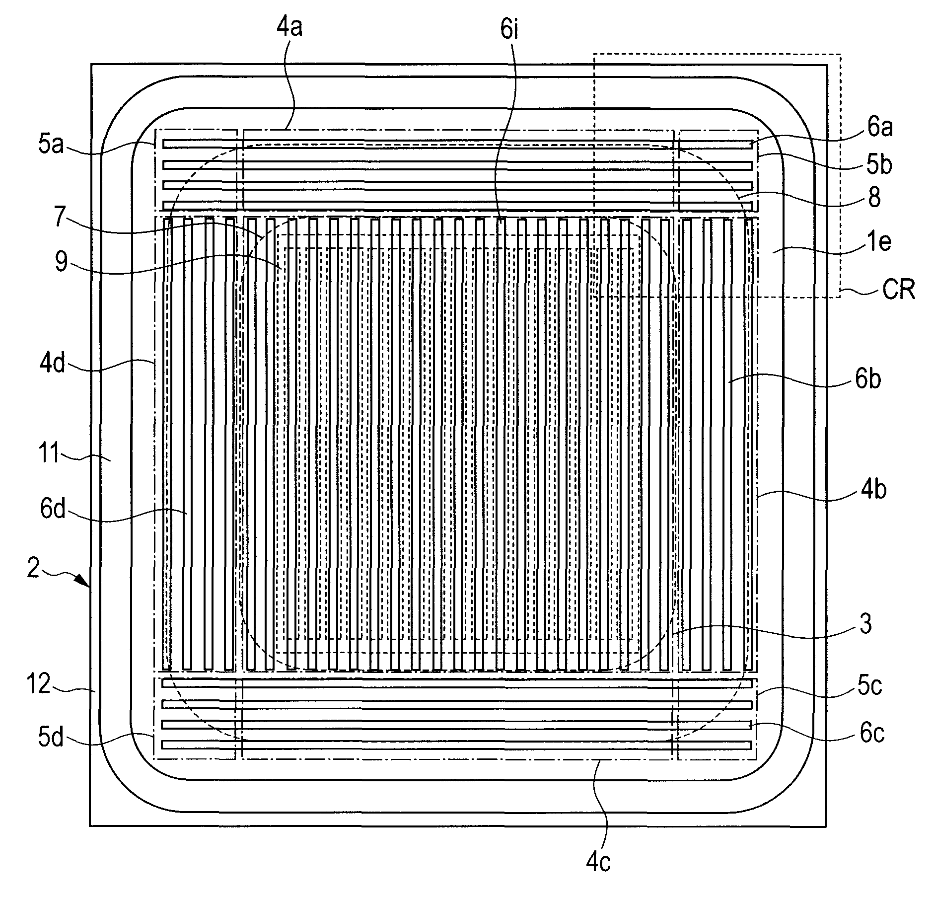
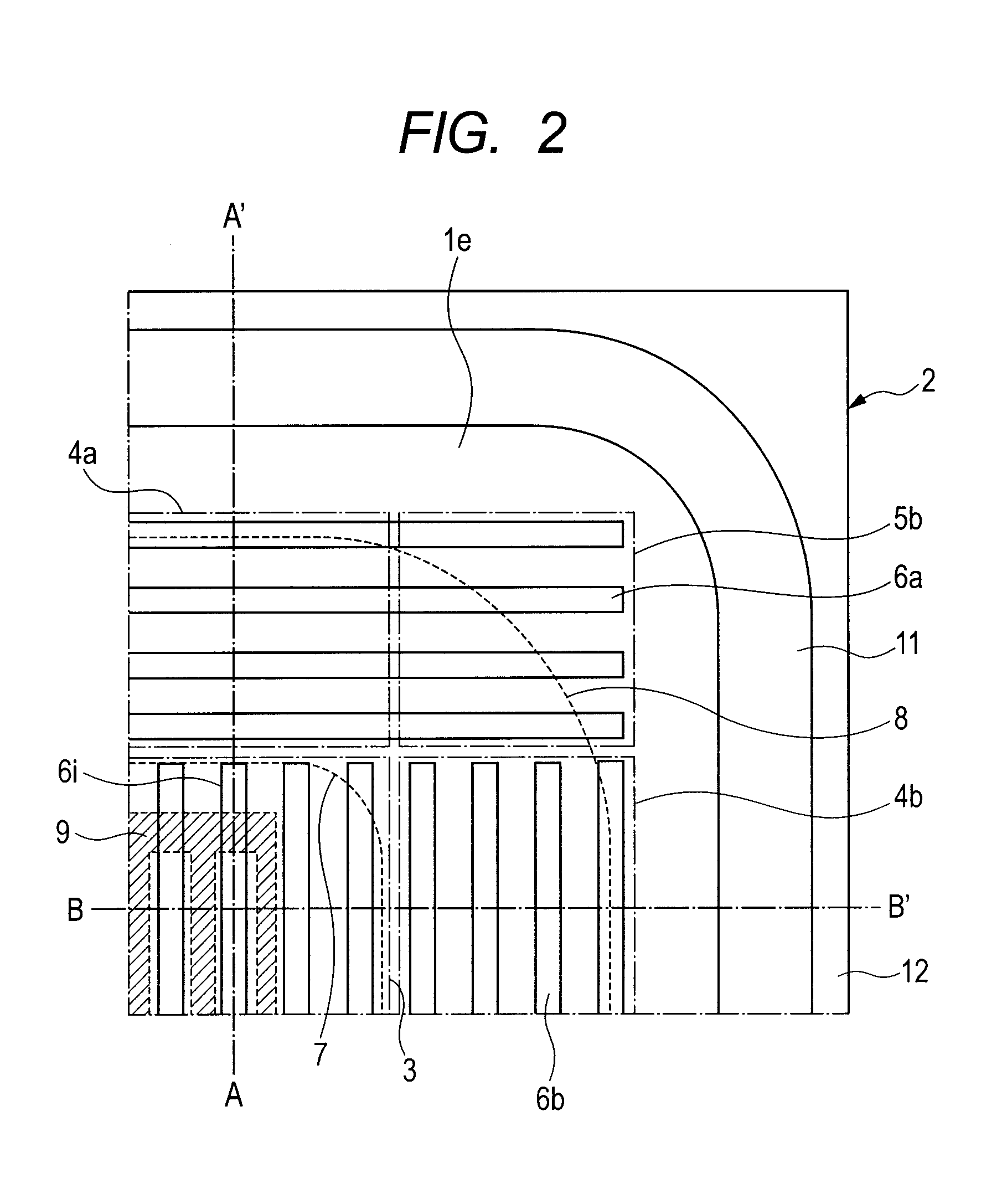
1. Description of the Device Structure (2D Resurf Structure) of a Power MOSFET as a Semiconductor Device According to the Invention (See Mainly FIGS. 1 to 4).

[0104]Although the super junction structure is also a kind of resurf structure, the resurf structure described in this section is the resurf structure for a P− type surface layer formed over a bulk super junction structure surface of the bulk in a cell peripheral region. In the cell peripheral region, P type columns extend parallel to corresponding sides of the cell region, and in terms of the degree of freedom in electric field directions in the depletion layer extending to the P− type surface layer, the structure also has a 2-degree-of-freedom, specifically the direction from the back surface of the substrate to its front surface and the direction from a chip edge toward the inside of the device main surface; thus this type of resurf structure is called a 2D resurf structure.

[0105]Next, the function of the 2D resurf structure...

second embodiment

3. Description of the Device Structure (3D Resurf Structure) of a Power MOSFET as a Semiconductor Device According to the Invention (See Mainly FIGS. 19 to 21)

[0127]In the resurf structure described in this section, P type columns extend perpendicularly to corresponding sides of the cell region in the cell peripheral region, so in terms of the degree of freedom in electric field directions in the depletion layer extending to the P− type surface layer, the structure has a 3-degree-of-freedom, specifically the direction parallel to a corresponding side of the cell region, the direction from the back surface of the substrate to its front surface, and the direction from the chip edge toward the inside of the device main surface; thus this type of resurf structure is called a 3D resurf structure. The basic configuration of the device is almost the same as that of the device described in Section 1 and basically, only aspects which are different from it will be described in this and subseq...


PUM


Abstract

A semiconductor device which solves the following problem of a super junction structure: due to a relatively high concentration in the body cell region (active region), in peripheral areas (peripheral regions or junction end regions), it is difficult to achieve a breakdown voltage equivalent to or higher than in the cell region through a conventional junction edge terminal structure or resurf structure. The semiconductor device includes a power MOSFET having a super junction structure formed in the cell region by a trench fill technique. Also, super junction structures having orientations parallel to the sides of the cell region are provided in a drift region around the cell region.

Description

CROSS-REFERENCE TO RELATED APPLICATIONS[0001]The disclosure of Japanese Patent Application No. 2009-263600 filed on Nov. 19, 2009 including the specification, drawings and abstract is incorporated herein by reference in its entirety.BACKGROUND OF THE INVENTION[0002]The present invention relates to semiconductor devices (or semiconductor integrated circuit devices) and a cell peripheral layout technique or a breakdown voltage enhancement technique in a method for manufacturing a semiconductor device (or semiconductor integrated circuit device).[0003]Japanese Unexamined Patent Publication No. 2007-116190 and U.S. Patent Publication 2005-098826 disclose various structures relating to layout of the vicinity of a cell region in a power MOSFET (Metal Oxide Semiconductor Field Effect Transistor) with a super junction structure which is manufactured by a multi-epitaxial technique or a trench insulating film filling technique (implantation of ions into trenches). These structures include P− ...

Claims


Application Information

Patent Timeline
Patent Type & Authority Patents(United States)
IPC IPC(8): H01L29/06
CPCH01L27/088H01L29/6634H01L29/66727H01L29/063H01L29/0634H01L29/0696H01L29/402H01L29/7811H01L29/41766H01L29/41741H01L29/0615H01L29/7396H01L29/0638H01L29/0619H01L29/1095H01L29/7395
Inventor TAMAKI, TOMOHIRONAKAZAWA, YOSHITOEGUCHI, SATOSHI
Owner RENESAS ELECTRONICS CORP
Why Eureka
Try Eureka