Semiconductor device and manufacturing method thereof
a semiconductor device and manufacturing method technology, applied in the direction of semiconductor devices, basic electric elements, electrical appliances, etc., can solve the problems of high parasitic capacitance, insufficient preventive malfunction, and high risk of malfunction, so as to reduce the displacement current generated by dv/dt noise, prevent the malfunction of the semiconductor device, and increase the lateral resistance
- Summary
- Abstract
- Description
- Claims
- Application Information
AI Technical Summary
Benefits of technology
Problems solved by technology
Method used
Image
Examples
working example 1
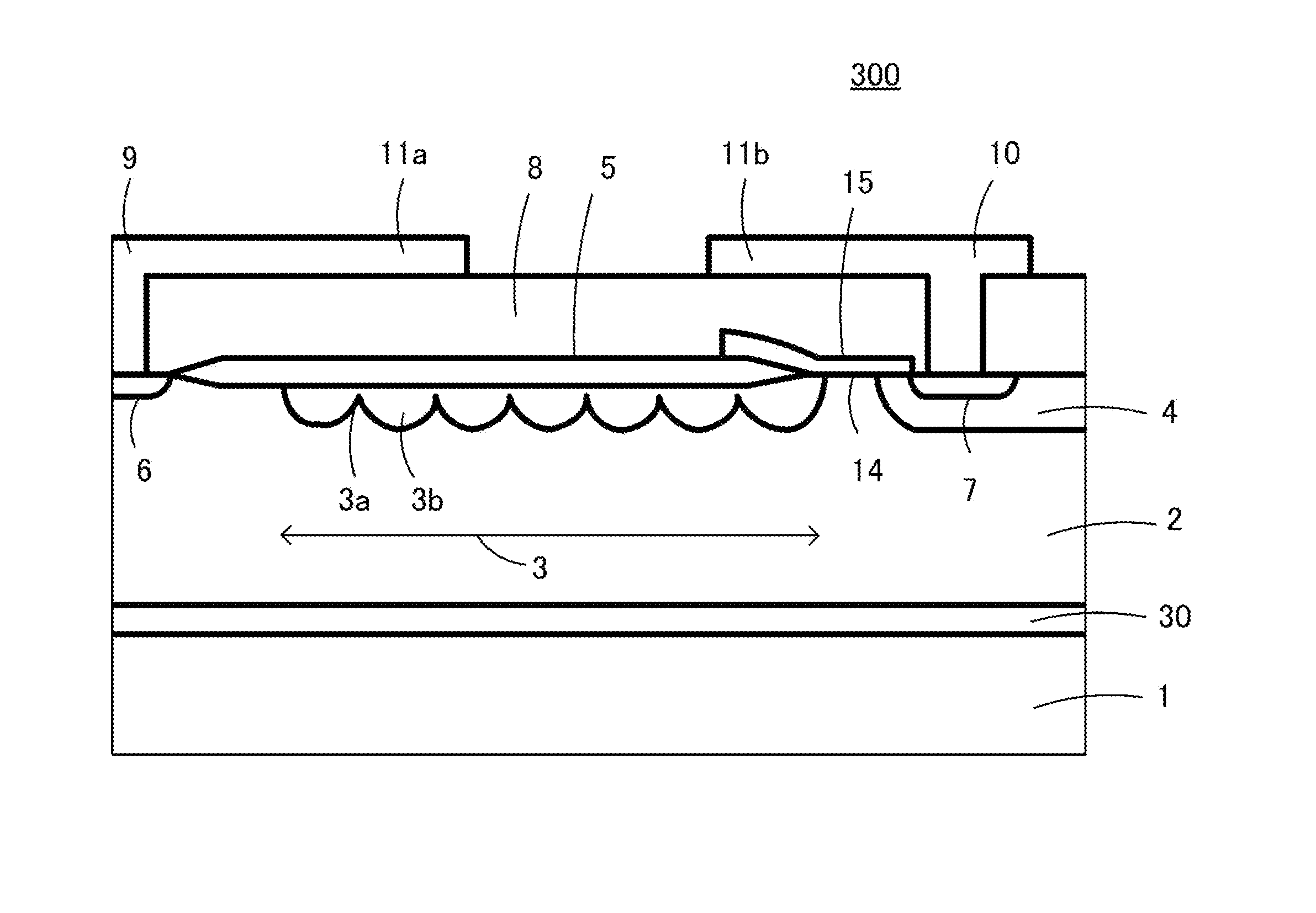
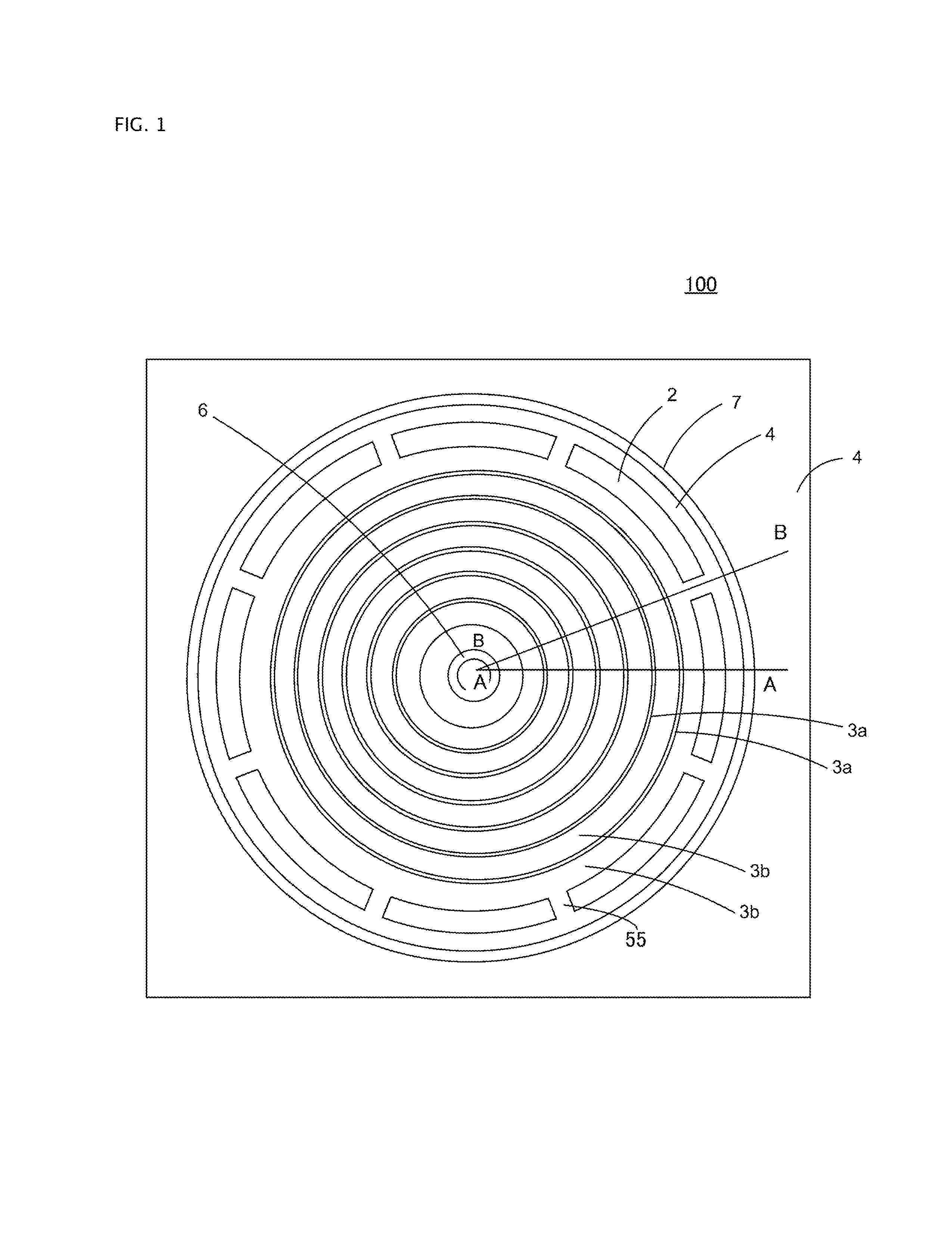
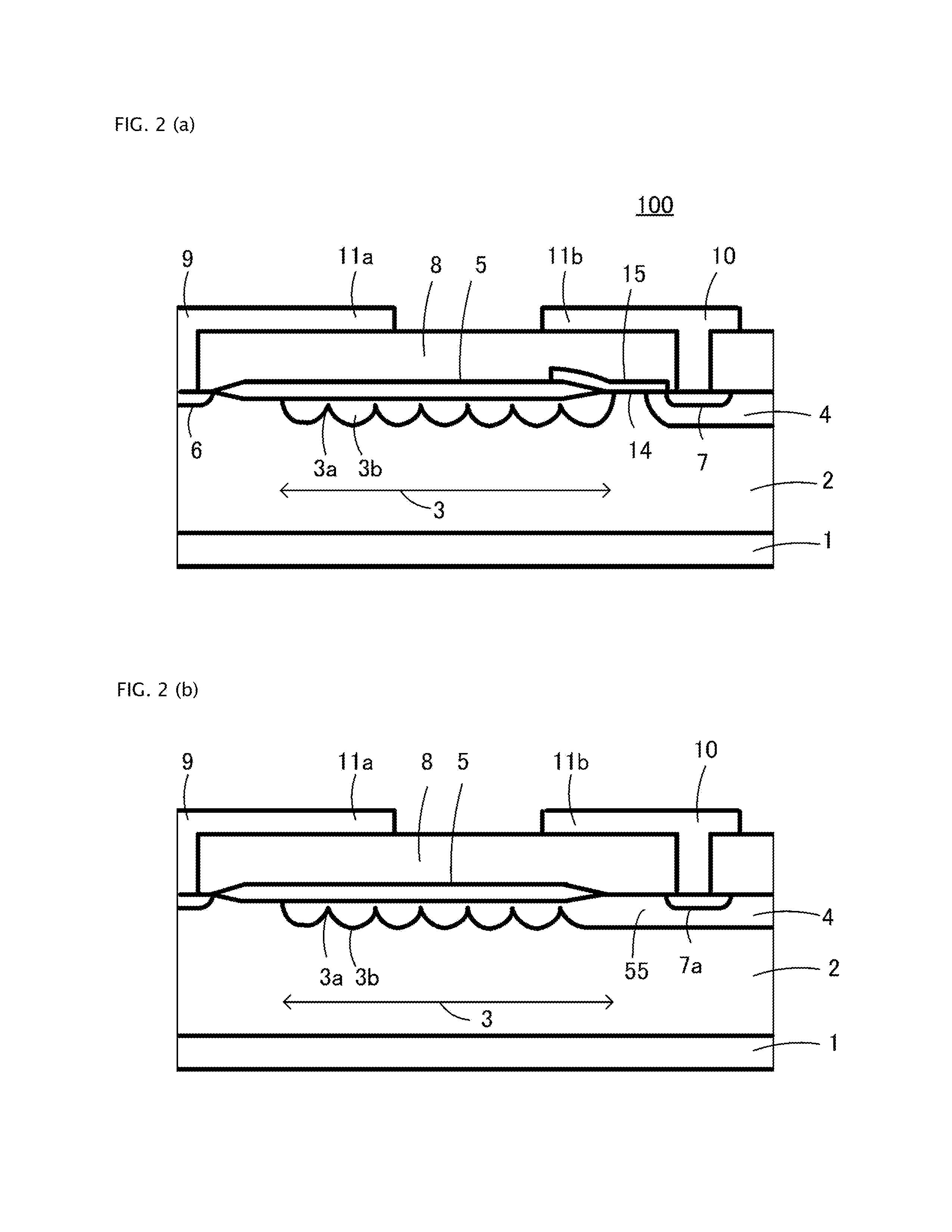
[0058]FIGS. 1 to 2B are configuration diagrams of a semiconductor device according to a first working example of the invention, wherein FIG. 1 is a main portion plan view, FIG. 2A is a main portion sectional view taken along line A-A of FIG. 1, and FIG. 2B is a main portion sectional view taken along line B-B of FIG. 1. FIGS. 1 to 2B show a MOSFET used as a level shifter formed in an HVIC described in FIG. 16 or 18. The MOSFET is formed in a low potential region, and drain electrode 9 is connected to a high potential region by a bonding wire (not shown). Also, the outer peripheral end of p-type well region 4 acting as the low potential region is shown in a circular shape here but, not being limited to this, expands outward to any size.
[0059]Semiconductor device 100 includes n-type semiconductor layer 2 formed on a surface layer of p-type semiconductor substrate 1 and p-type diffusion layer 3 formed on a surface layer of n-type semiconductor layer 2. N-type semiconductor layer 2 may ...
working example 2
[0084]FIGS. 7 to 9B are configuration diagrams of a semiconductor device 200 according to a second working example of the invention, wherein FIG. 7 is a main portion plan view, FIG. 8 is an enlarged main portion plan view of an F portion in FIG. 7, FIG. 9A is a main portion sectional view taken along line C-C of FIG. 8, and FIG. 9B is a main portion sectional view taken along line D-D of FIG. 8.
[0085]In FIG. 7, high voltage isolation structure 20, having an annular zonal shape with a fixed width in a plan view, encloses high potential region 18. The plan-view outline of high voltage isolation structure 20 includes linear portions 16 and corner portions 17 having a curved shape with a fixed curvature. The width of high voltage isolation structure 20 is approximately 200 μm, and the curvature radius of corner portions 17 is approximately 80 μm.
[0086]The difference from semiconductor device 100 of the first working example is that a level shift MOSFET is formed in high voltage isolatio...
working example 3
[0089]FIGS. 10A to 10C, showing a method of manufacturing a semiconductor device according to a third working example of the invention, are main portion manufacturing process sectional views shown in a process order. Herein, FIGS. 10A to 10C show a process of manufacturing the semiconductor device 200 of the second working example. The manufacturing process sectional views correspond to the sectional view of FIG. 9A. Also, herein, FIGS. 10A to 10C show steps of using a shielding mask to form the p-type low concentration regions 3a and p-type high concentration regions 3b configuring p-type diffusion layer 3.
[0090]Resist mask 21 acting as a shielding mask is formed on a surface of n-type semiconductor layer 2 (FIG. 10A). Next, boron 22 is ion implanted. The dose amount is set to an optimal value (a dose amount wherein a breakdown voltage is highest) satisfying double-RESURF conditions (FIG. 10B).
[0091]After resist mask 21 is removed, a heat treatment is performed to form p-type high ...
PUM
 Abstract
Description
Claims
Application Information


