Partitioned reaction container for manufacturing capacitor element including openable and closable passage
a reaction container and capacitor technology, applied in capacitor manufacture, capacitor manufacturing, electrolytic capacitors, etc., can solve the problems of difficult to form a uniform semiconductor layer on the inside of each conductive member, difficult to evenly pass electric current through a plurality of conductive members, and difficult to evenly pass electric current through them. the effect of forming a uniform semiconductor layer and a container can be further strengthened
- Summary
- Abstract
- Description
- Claims
- Application Information
AI Technical Summary
Benefits of technology
Problems solved by technology
Method used
Image

Examples
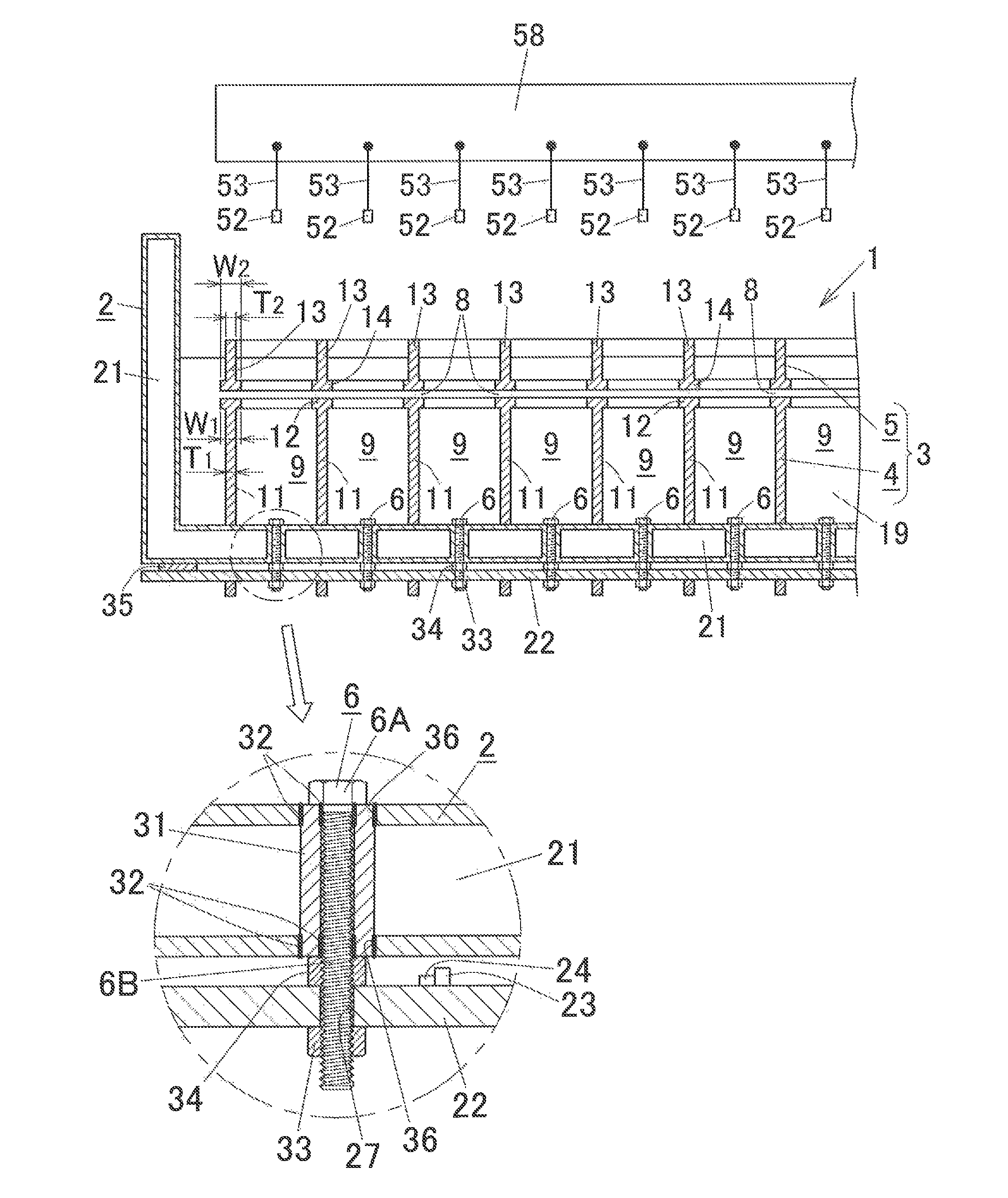
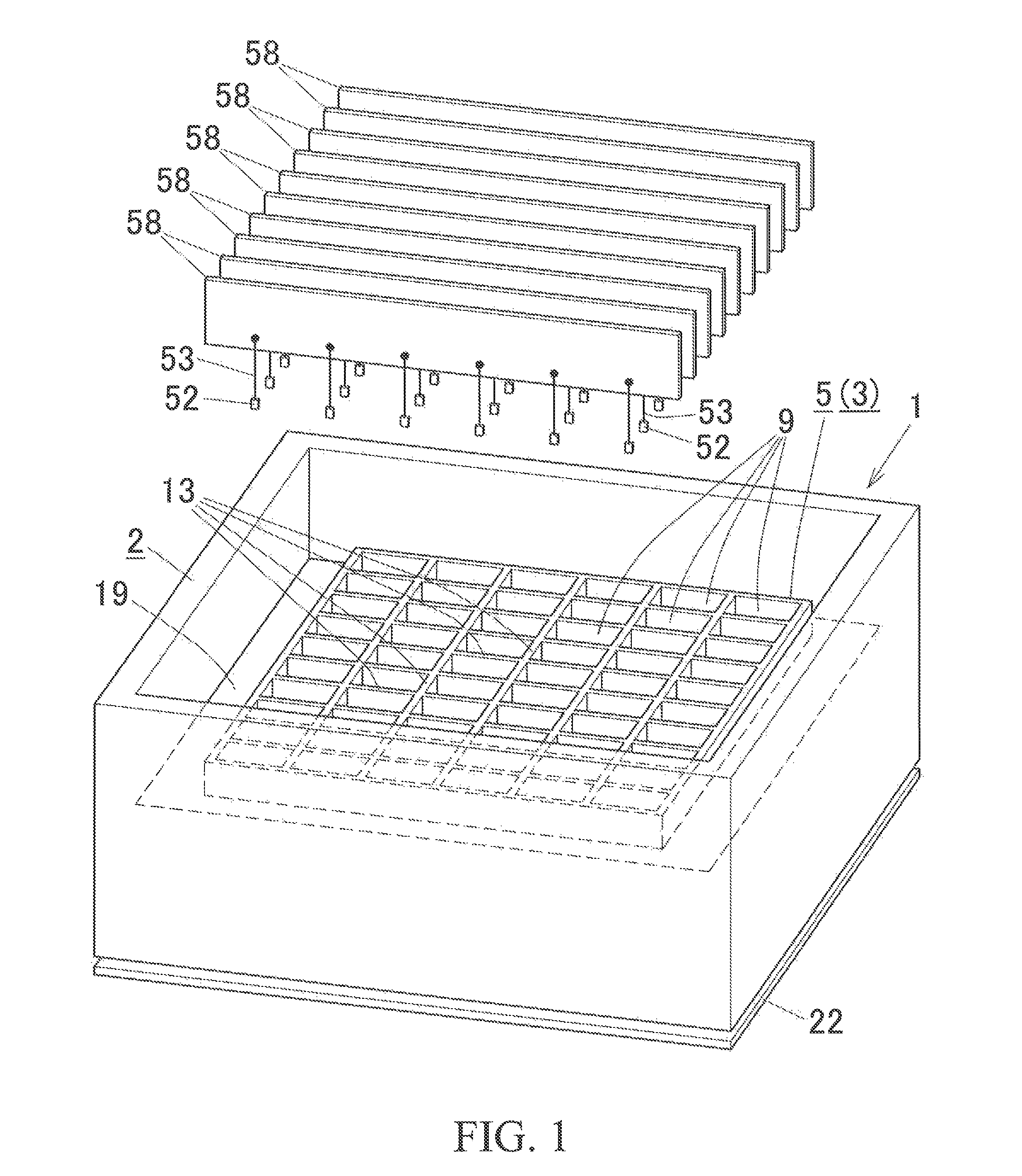
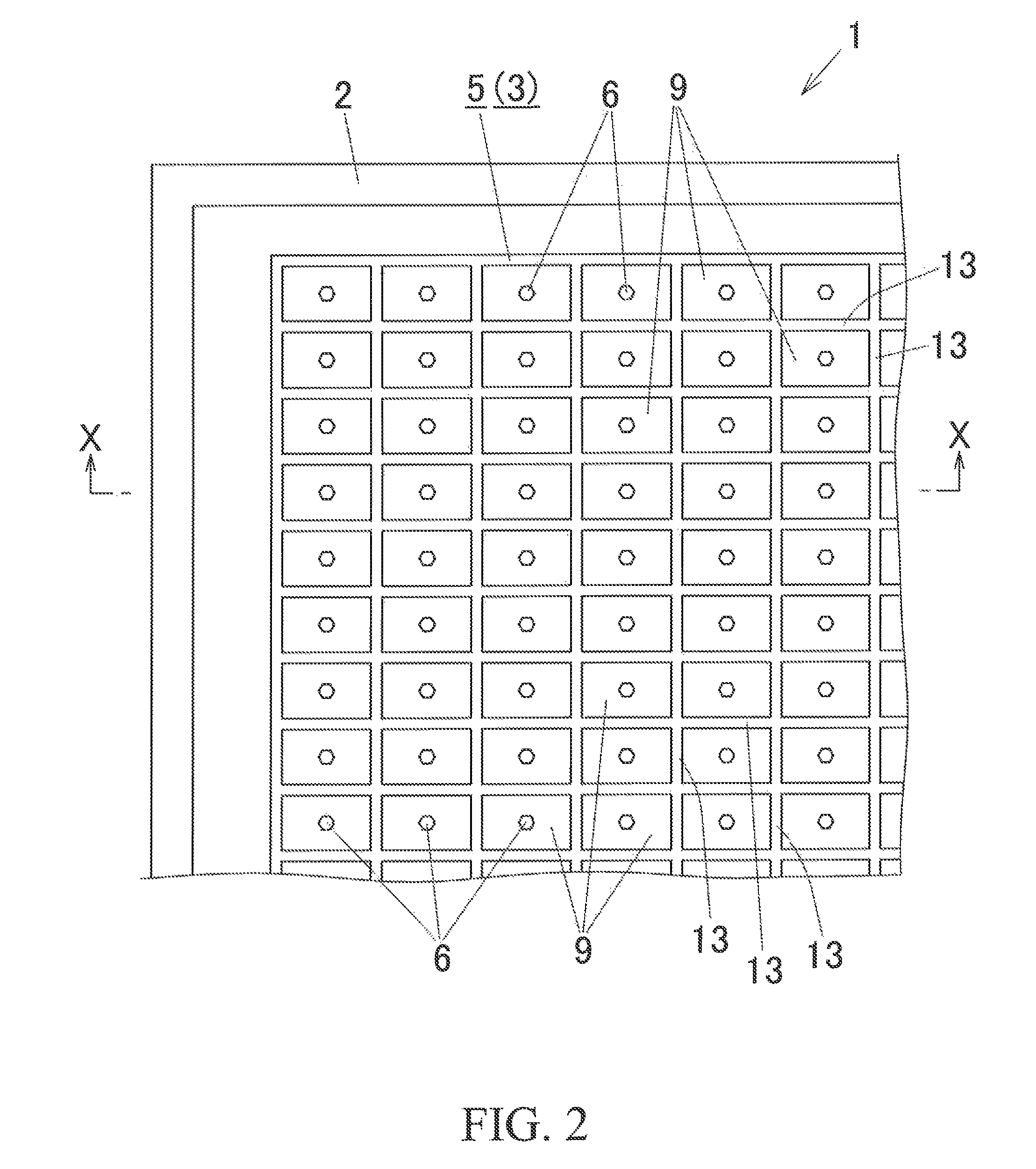
example 1
Production of Anode Member (Conductive Member) 52
[0121]Niobium power having an average particle diameter of 125 μm was obtained by granulating niobium primary powder (average grain diameter of 0.17 μm) obtained by pulverizing a niobium (Nb) ingot using the hydrogen brittleness. Next, the obtained niobium powder was partially nitrided to obtain partially nitrided niobium powder (oxygen content: 6,500 mass ppm, nitrogen content: 7,600 ppm, CV value: 280,000 μF·V / g). The partially nitrided niobium powder was molded together with a niobium wire (lead wire) having a diameter of 0.29 mm, and then vacuum sintered at 1,240° C. to obtain a sintered body (anode member) 52 of a rectangular parallelepiped shape having a length of 2.3 mm, a width of 1.7 mm, a thickness of 1.0 mm, and a mass of 15.2 mg. The niobium lead wire 53 was buried approximately in the center of the surface of 1.7 mm×1.0 mm, and integrally formed with the sintered body 52 such that the lead wire 53 was outwardly extended f...
PUM
| Property | Measurement | Unit |
|---|---|---|
| grain diameter | aaaaa | aaaaa |
| particle diameter | aaaaa | aaaaa |
| thickness | aaaaa | aaaaa |
Abstract
Description
Claims
Application Information