Structure of high electron mobility transistor growth on Si substrate and the method thereof

a high electron mobility, transistor technology, applied in the direction of basic electric elements, semiconductor devices, electrical equipment, etc., can solve the problems of high cost of mbe, difficult difficulty in using lep to manufacture epitaxy layers with high doping concentration or thin thickness, etc., to reduce the thickness of elements and reduce the quality of films. , the effect of reducing the thickness of elements

Inactive Publication Date: 2014-08-05
NAT CHIAO TUNG UNIV
View PDF6 Cites 2 Cited by
  • Summary
  • Abstract
  • Description
  • Claims
  • Application Information

AI Technical Summary

Benefits of technology

[0019]The present invention uses Ge film to protect the substrate (for example, Si substrate) so as to prevent to generate silicon oxide (SiO2) and decrease the quality of the film when it uses MOCVD to form the transistor substrate. If the Ge film directly grows on the substrate, the dislocation and defect will generate on the Ge film. Therefore, it is necessary to grow the metamorphic structure on the Ge film so as to use the metamorphic structure to prevent the dislocation of the Ge film growing upward and lower the thickness of element and manufacture cost.

Problems solved by technology

However, it is difficult to use LEP to manufacture the epitaxy layer with high doping concentration or the thin thickness.
However, the cost of MBE is also higher.
The Metal-Organic Chemical Vapor Deposition (MOCVD) which has various chemical change and great technology difficult.
However, the manufacture cost of MOCVD is lower and the production of the MOCVD is higher than the MBE.
However, the substrate with InP or GaAs is very expensive and has bad performance of mechanical, and it will cause that MHEMT is not easy to grow on the larger substrate and is also rapidly increasing in prices of cost.
Therefore, the manufacture cost of the SixGe1-x substrate is higher and the MHEMT manufactured also has the deep thickness, and the mismatch and bug are also easy generated in growing of the GaAs.

Method used


Image

  • Structure of high electron mobility transistor growth on Si substrate and the method thereof
  • Structure of high electron mobility transistor growth on Si substrate and the method thereof
  • Structure of high electron mobility transistor growth on Si substrate and the method thereof

Examples


Embodiment Construction

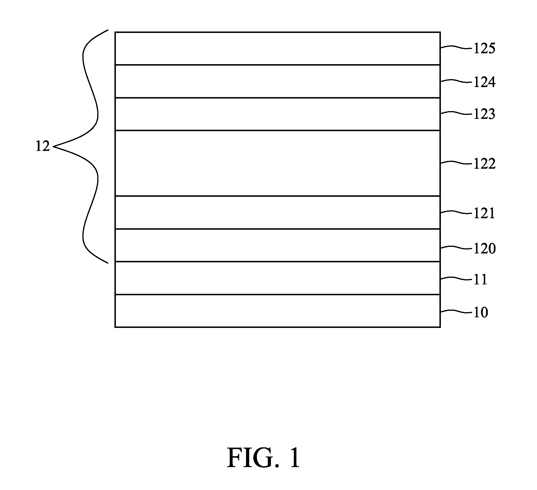
[0024]FIG. 1 is a schematic diagram showing a structure of high electron mobility transistor growth on Si substrate according to one embodiment of the present invention. The structure comprises:

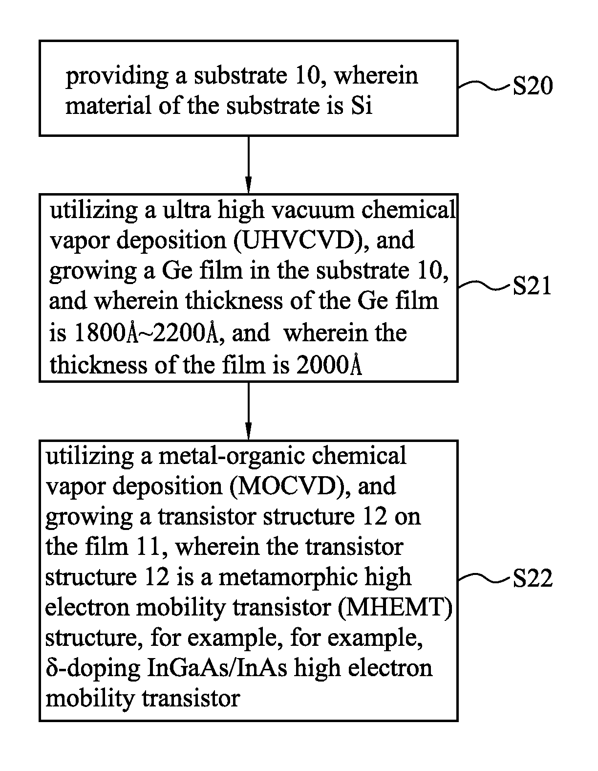
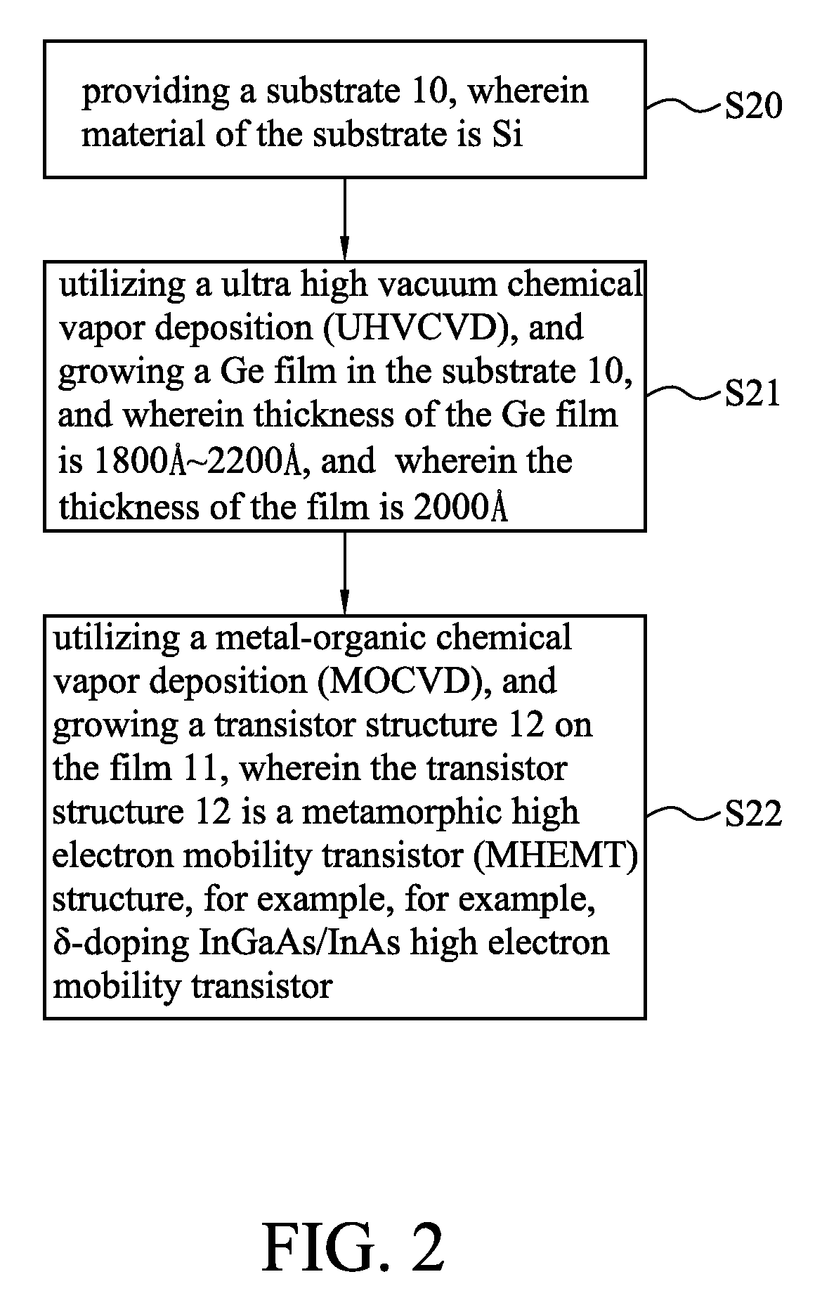
[0025]a substrate 10, wherein material of the substrate is Si;

[0026]a film 11, wherein material of the film is Ge and the film grows on the substrate 10 and the film's thickness is 1800 Ř2200 Å by utilizing a ultra high vacuum chemical vapor deposition (UHVCVD), and wherein the optimal thickness is 2000 Å;

[0027]a transistor structure 12, wherein the transistor structure 12 is a metamorphic high electron mobility transistor (MHEMT) structure and the transistor structure 12 grows on the film by utilizing a metal-organic chemical vapor deposition (MOCVD).

[0028]Specifically, the transistor structure 12 further comprises:

[0029]a buffer layer 120, wherein material of the buffer layer 120 is III-V Compound (for example, InAlAs):

[0030]a channel layer 121, growing on the buffer layer 120, wherein mat...


PUM


Abstract

A structure of high electron mobility transistor growth on Si substrate and the method thereof, in particular used for the semiconductor device manufacturing in the semiconductor industry. The UHVCVD system was used in the related invention to grow a Ge film on Si substrate then grow the high electron mobility transistor on the Ge film for the reduction of buffer layer thickness and cost. The function of the Ge film is preventing the formation of silicon oxide when growing III-V MHEMT structure in MOCVD system on Si substrate. The reason of using MHEMT in the invention is that the metamorphic buffer layer in MHEMT structure could block the penetration of dislocation which is formed because of the very large lattice mismatch (4.2%) between Ge and Si substrate.

Description

TECHNICAL FIELD[0001]The present disclosure relates to a structure of high electron mobility transistor growth on si substrate and the method thereof, and more particularly, to apply in the semiconductor manufacturing and it utilizes a ultra high vacuum chemical vapor deposition (UHVCVD) to grow a Ge film on the Si substrate, and utilizes a metamorphic high electron mobility transistor (MHEMT) to grow a transistor structure on the Ge film so as to decrease the thickness of the element and the manufacture cost.TECHNICAL BACKGROUND[0002]In recent years, the high-frequency microwave epitaxy chip is used in wide range, for example, mobile communication, global position system, wireless network etc. Therefore, the high-frequency element development has become the irresistible tide of the day. Specifically, the compound semiconductor epitaxial fabrication is one of the most development technologies.[0003]There are three main types of the compound semiconductor epitaxial fabrication: Large...

Claims


Application Information

Patent Timeline
Patent Type & Authority Patents(United States)
IPC IPC(8): H01L21/20H01L21/36
CPCH01L29/7784H01L29/267
Inventor YI CHANG, EDWARDTANG, SHIH-HSUANLIN, YUEH-CHIN
Owner NAT CHIAO TUNG UNIV
Why Eureka
Try Eureka