Bit line structure, semiconductor device and method of forming the same

a technology of bit line structure and semiconductor device, which is applied in the direction of semiconductor device, semiconductor/solid-state device details, electrical apparatus, etc., can solve the problems of junction leakage, and reduced current of memory cells, so as to avoid over-high bit line loading and reduce bit line resistance

Active Publication Date: 2014-08-19
MACRONIX INT CO LTD
View PDF6 Cites 9 Cited by
  • Summary
  • Abstract
  • Description
  • Claims
  • Application Information

AI Technical Summary

Benefits of technology

[0008]Accordingly, the present invention provides a semiconductor device, in which the conductive layers serve as bit lines to reduce the bit line resistance and avoid over-high bit line loading.
[0009]The present invention further provides a method of forming a semiconductor device. The process is simple and easy, and the formed semiconductor device has lower bit line resistance.
[0010]The present invention also provides a bit line structure to avoid the short channel effect and the junction leakage problem.
[0027]In view of the above, the semiconductor device of the present invention uses the conductive layers as bit lines, so as to reduce the bit line resistance and avoid over-high bit line loading. Therefore, the read current loading is reduced, the threshold voltage variation is decreased, and the programming speed is increased. Further, the method of forming the semiconductor device of the present invention is simple and easy. The semiconductor device of the present invention can be formed with the existing manufacturing equipment, so that the competitive advantage can be achieved easily. In addition, the bit line structure of the present invention can avoid the short channel effect and the junction leakage problem.

Problems solved by technology

However, a narrower width of the bit lines leads to higher resistance, so that the current of the memory cell is reduced and the over-high bit line loading is caused.
If the junction depth of the bit lines is increased to resolve the higher resistance of the bit lines, not only the short channel effect is generated, the problem of junction leakage also occurs.
If a high concentration of dopant is used to form a shallow junction of the bit lines to obviate the short channel effect and the junction leakage problem caused by the deep junction, the overloading problem of the bit lines remains unresolved due to the limitation of the solid-state solubility.

Method used


Image

  • Bit line structure, semiconductor device and method of forming the same
  • Bit line structure, semiconductor device and method of forming the same
  • Bit line structure, semiconductor device and method of forming the same

Examples


Embodiment Construction

[0032]Reference will now be made in detail to the present preferred embodiments of the invention, examples of which are illustrated in the accompanying drawings. Wherever possible, the same reference numbers are used in the drawings and the description to refer to the same or like parts.

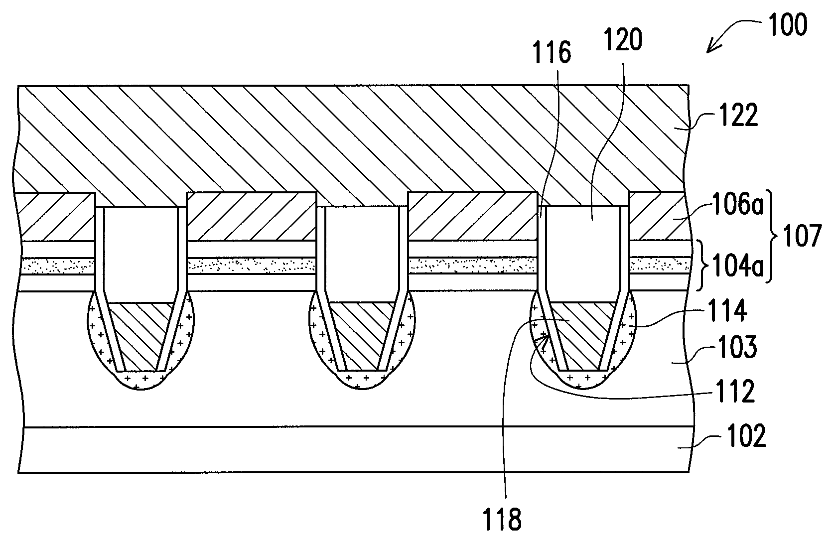
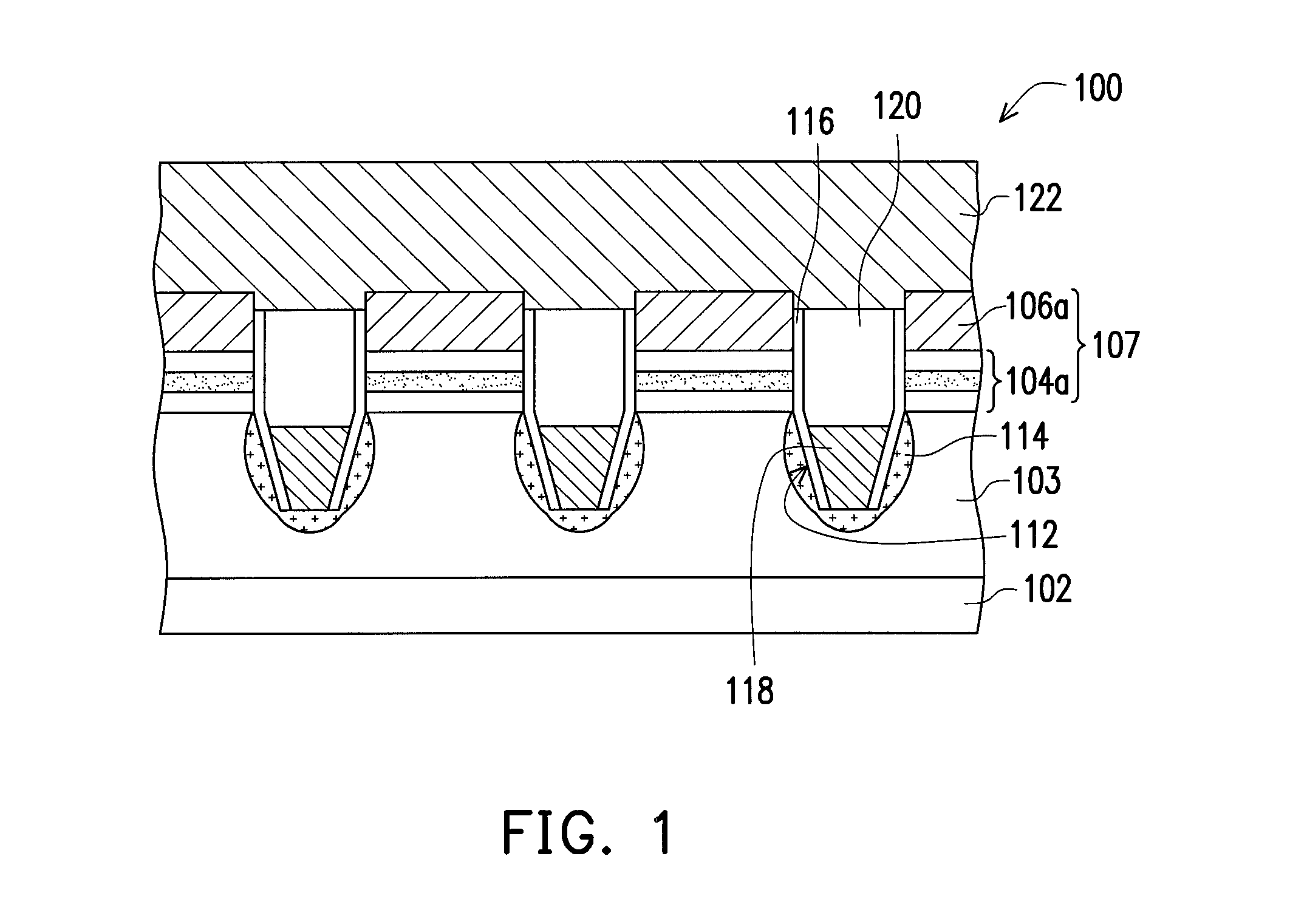
[0033]FIG. 1 schematically illustrates a cross-sectional view of a semiconductor device according to an embodiment of the present invention.

[0034]Referring to FIG. 1, a semiconductor device 100 of the present invention includes a substrate 102, a well region 103, a plurality of stacked gate structures 107, a plurality of doped regions 114, a plurality of liner layers 116, a plurality of conductive layers 118, a plurality of dielectric layers 120 and a plurality of word lines 122.

[0035]The substrate 102 may be a silicon substrate. The substrate 102 has a plurality of trenches 112 therein. The well region 103 is disposed in the substrate 102. The trenches 112 are disposed in the well region 103. Each d...


PUM


Abstract

A semiconductor device including a substrate, a plurality of stacked gate structures, a plurality of doped regions, a plurality of liner layers, a plurality of conductive layers, a plurality of dielectric layers and a plurality of word lines is provided. The substrate has a plurality of trenches therein. The stacked gate structures are on the substrate between the trenches. The doped regions are in the substrate at sidewalls or bottoms of the trenches. The liner layers are on at least a portion of sidewalls of the stacked gate structures and on sidewalls of the trenches. The conductive layers are in the trenches and electrically connected to the doped regions. The dielectric layers are on the conductive layers and between the stacked gate structures. The word lines are on the substrate and electrically connected to the stacked gate structures.

Description

CROSS-REFERENCE TO RELATED APPLICATION[0001]This application claims the priority benefit of Taiwan application serial no. 99104797, filed on Feb. 12, 2010. The entirety of the above-mentioned patent application is hereby incorporated by reference herein and made a part of specification.BACKGROUND OF THE INVENTION[0002]1. Field of Invention[0003]The present invention relates to a semiconductor method and a method of forming the same, and more generally to a non-volatile memory and a method of forming the same.[0004]2. Description of Related Art[0005]A non-volatile memory provides the property of multiple entries, retrievals and erasures of data, and is able to retain the stored information even when the electrical power is off. Therefore, a non-volatile memory is widely used in personal computers and consumer electronic products.[0006]As the level of integration of a non-volatile memory is getting higher, the critical dimension such as the width of bit lines is accordingly reduced. H...

Claims


Application Information

Patent Timeline
Patent Type & Authority Patents(United States)
IPC IPC(8): H01L29/788H01L21/74H01L27/115
CPCH01L27/11568H01L21/743H10B43/30
Inventor LEE, GUAN-DELIU, CHIEN-HUNGHUANG, SHOU-WEICHEN, YING-TSO
Owner MACRONIX INT CO LTD
Why Eureka
Try Eureka