Silicon carbide semiconductor device

a silicon carbide and semiconductor technology, applied in the direction of semiconductor devices, electrical apparatus, transistors, etc., can solve the problems of increased switching power loss, limited si device minimum power loss, slow switching, etc., and achieve small series resistance and wide safe operating area

Active Publication Date: 2014-09-09
SEMICON COMPONENTS IND LLC
View PDF25 Cites 14 Cited by
  • Summary
  • Abstract
  • Description
  • Claims
  • Application Information

AI Technical Summary

Problems solved by technology

The minimum power losses of these Si devices are, however, limited by the thick lowly doped drift region that is necessary to ensure high voltage blocking capability.
The thick drift region adds to the on-state resistance of the devices thus increasing the power losses during conduction and in bipolar Si devices there is a significant stored charge that causes slower switching and increased switching power losses.
The fundamental material properties of Si are a barrier to substantial reductions of the power losses, that become more and more limiting for the continuous downscaling of power electronic systems.
SiC pn diodes have the disadvantage that a forward voltage of close to 3 V has to be applied to give forward conduction and this means relatively high conduction power losses for pn diodes with moderate breakdown voltages.
The blocking capability is limited by avalanche breakdown of the base-collector junction if the base is designed with a doping dose high enough to avoid punch-through at voltages below the avalanche breakdown voltage.
The vertical BJT structure shown in FIG. 1b is most commonly used for SiC BJTs since diffusion of dopants cannot be used, and ion implantation has been found to create current gain degrading defects if it is performed in the active region of the bipolar junction transistor.

Method used


Image

  • Silicon carbide semiconductor device
  • Silicon carbide semiconductor device
  • Silicon carbide semiconductor device

Examples


Embodiment Construction

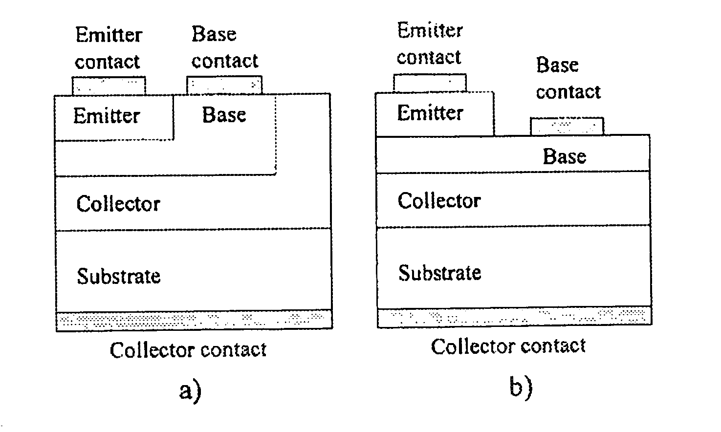
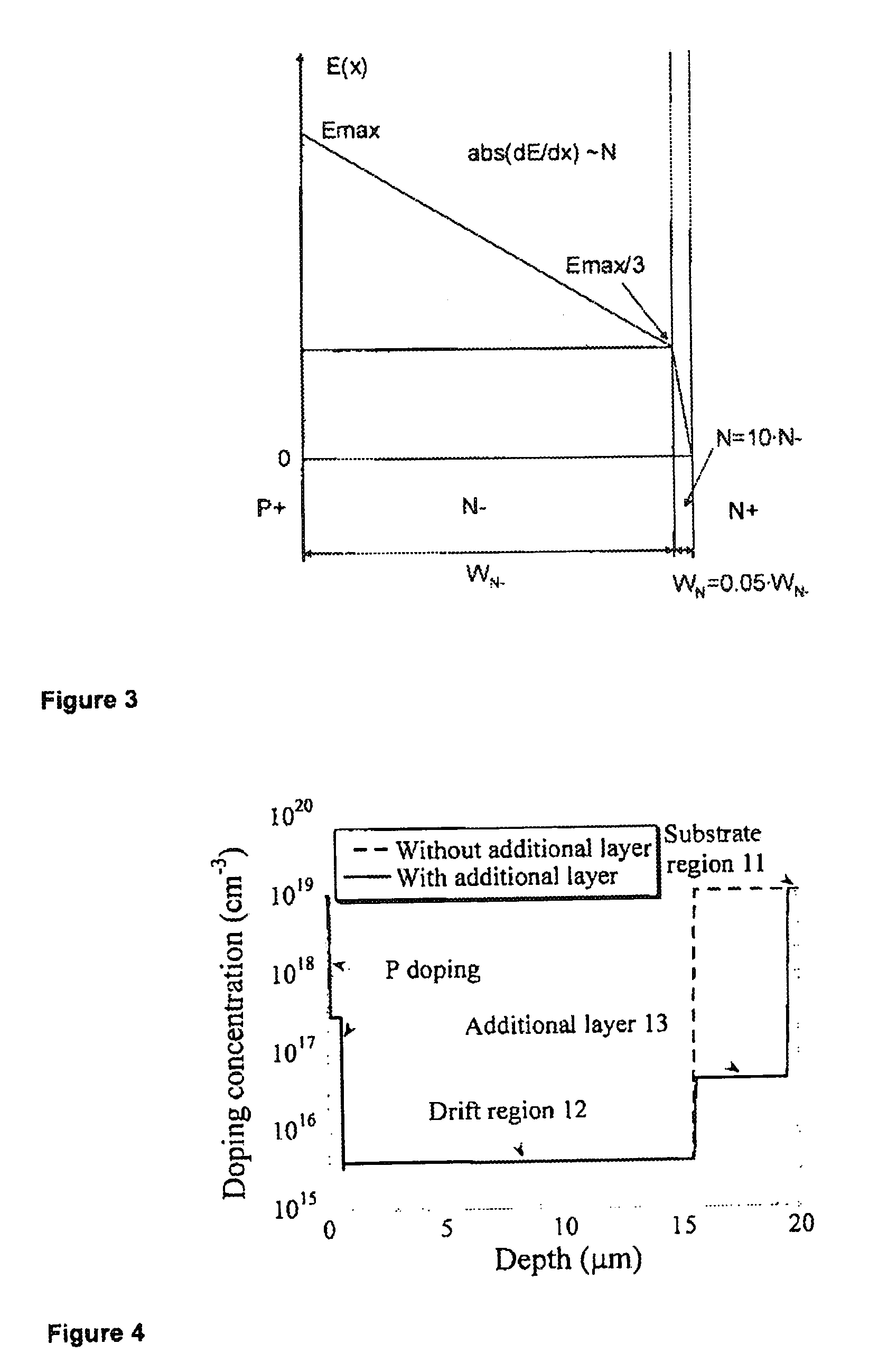
[0057]The present invention will now be described with reference to FIG. 4, where a silicon carbide bipolar junction transistor for power electronics applications, is described as an exemplifying embodiment of the invention.

[0058]FIG. 4 shows schematically a semiconductor device 1 in silicon carbide, with a highly doped substrate region 11 and a drift region 12.

[0059]An additional layer 13 is positioned between the highly doped substrate region 11 and the drift region 12, the additional layer 13 providing a wider safe operating area at high voltages with subsequently high current densities.

[0060]The additional layer 13 has the same type of doping as the substrate region 11 and the drift region 12, and the doping concentration in the additional layer 13 is higher than the doping concentration in the drift region 12 and lower than the doping concentration in the substrate region 11.

[0061]The presentment invention teaches that doping concentration of the additional layer 13 can be smal...


PUM


Abstract

The present invention relates to a semiconductor device (1) in silicon carbide, with a highly doped substrate region (11) and a drift region (12). The present invention specifically teaches that an additional layer (13) is positioned between the highly doped substrate region (11) and the drift region (12), the additional layer (13) thus providing a wide safe operating area at subsequently high voltages and current densities.

Description

[0001]This application is the U.S. national phase under 35 U.S.C. 371 of International Application No. PCT / SE2008 / 050408 filed 10 Apr. 2008, which claims priority to Sweden Application No. 0700896-4 filed 11 Apr. 2007, the entire contents of each of which are hereby incorporated by reference.FIELD OF INVENTION[0002]The present invention relates to a semiconductor device in silicon carbide, with a highly doped substrate region and a drift region.DESCRIPTION OF BACKGROUND ART[0003]Silicon carbide (SiC) has excellent properties for fabrication of power semiconductor devices. SiC has due to its wide bandgap nearly ten times higher critical field strength than silicon and the wide bandgap also provides the possibility for devices that can operate at high temperatures. The thermal conductivity of SiC is also 2-3 times higher than for Si and this improved heat transport means that SiC devices can operate at higher power densities without being overheated.[0004]Power switching transistors a...

Claims


Application Information

Patent Timeline
Patent Type & Authority Patents(United States)
IPC IPC(8): H01L29/15H01L29/06H01L29/08H01L29/16H01L29/36H01L29/66H01L29/73H01L29/868
CPCH01L29/73H01L29/36H01L29/66068H01L29/868H01L29/0821H01L29/0615H01L29/1608
Inventor DOMEIJ, MARTIN
Owner SEMICON COMPONENTS IND LLC
Why Eureka
Try Eureka