
Polishing pad and method of producing semiconductor device

a technology of polishing pad and semiconductor, which is applied in the direction of flexible wheel, manufacturing tools, lapping machines, etc., can solve the problems of judging the planarity of the surface waste of treatment time of the test wafer and the cost of treatment, and difficult to accurately predict the processing results without actual processing of the product, so as to reduce the planarity of the object, improve the polishing effect, and reduce the strength of the polishing region

Inactive Publication Date: 2014-09-30
ROHM & HAAS ELECTRONICS MATERIALS CMP HLDG INC
View PDF46 Cites 11 Cited by
  • Summary
  • Abstract
  • Description
  • Claims
  • Application Information

AI Technical Summary

Benefits of technology

The patent is about improving the accuracy of polishing and film thickness measurement by using a polishing pad with a high light-transmissivity. The specific gravity of the foam used in the pad should be between 0.5 and 1.0 g / cm3 to achieve optimal results. If the specific gravity is too low, the surface of the polishing region becomes weaker, leading to lower planarity of the object being polished. On the other hand, if the specific gravity is too high, the number of fine cells on the surface of the pad decreases, but the rate of polishing tends to decrease.

Problems solved by technology

When such CMP is conducted, there is a problem of judging the planarity of wafer surface.
In this method, however, the treatment time of a test wafer and the cost for the treatment are wasteful, and a test wafer and a product wafer not subjected to processing are different in polishing results due to a loading effect unique to CMP, and accurate prediction of processing results is difficult without actual processing of the product wafer.
In high integration and micronization in production of semiconductors in the future, the wiring width of an integrated circuit is expected to be further decreased, for which highly accurate optical endpoint detection is necessary, but the conventional window for endpoint detection does not have sufficiently satisfactory accuracy in a broad wavelength range.
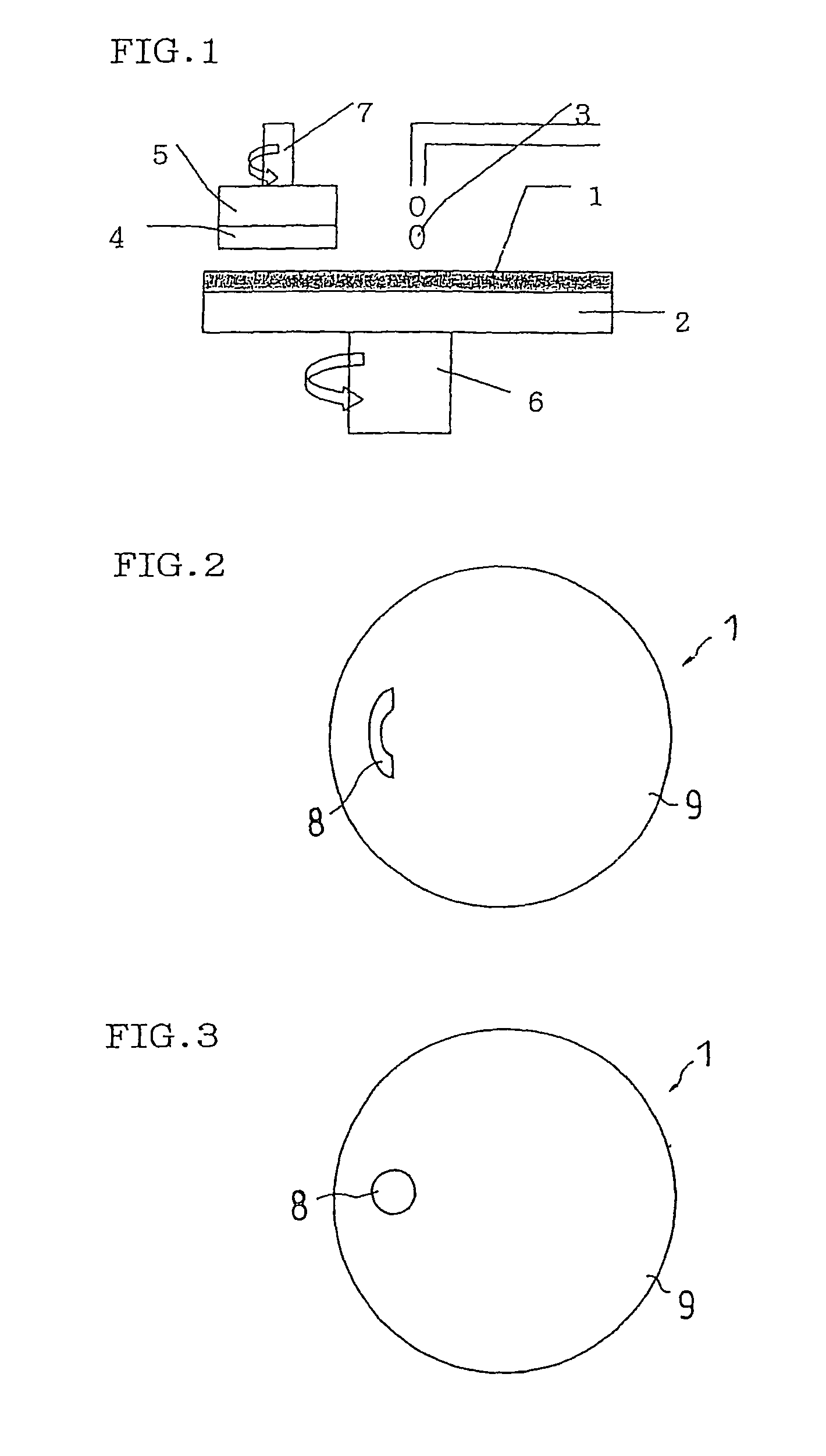
In the case of the window having the shape described above, however, the window contacts intensively with only a part of a wafer during polishing the wafer, and thus there is a problem that uneven polishing occurs between a portion contacting with the window and a portion not contacting with the window.
There is also a problem that an obtainable polishing profile is that of a limited portion contacting with the window.

Method used


Image

  • Polishing pad and method of producing semiconductor device
  • Polishing pad and method of producing semiconductor device
  • Polishing pad and method of producing semiconductor device

Examples


production example 1

[0168]125 parts by weight of polyester polyol (number-average molecular weight 2440) consisting of adipic acid and hexane diol were mixed with 31 parts by weight of 1,4-butane diol, and the temperature of the mixture was regulated at 70° C. To this mixture were added 100 parts by weight of 4,4′-diphenylmethane diisocyanate previously regulated at a temperature of 70° C., and the mixture was stirred for about 1 minute. The mixture was poured into a container kept at 100° C. and post-cured at 100° C. for 8 hours to prepare polyurethane resin. The prepared polyurethane resin was used to prepare a light-transmitting region (length 57 mm, width 19 mm, thickness 1.25 mm) by injection molding. The light transmittance of the prepared light-transmitting region and the rate of change thereof are shown in Table 1.

production example 2

[0169]A light-transmitting region (length 57 mm, width 19 mm, thickness 1.25 mm) was prepared in the same manner as in Production Example 1 except that 77 parts by weight of polyester polyol (number-average molecular weight 1920) consisting of adipic acid and hexane diol was used, and the amount of 1,4-butane diol was changed to 32 parts by weight. The light transmittance of the prepared light-transmitting region and the rate of change thereof are shown in Table 1.

production example 3

[0170]A light-transmitting region (length 57 mm, width 19 mm, thickness 1.25 mm) was prepared in the same manner as in Production Example 1 except that 114 parts by weight of polytetramethylene glycol (number-average molecular weight 890) was used as the polyol, and the amount of 1,4-butane diol was changed to 24 parts by weight. The light transmittance of the prepared light-transmitting region and the rate of change thereof are shown in Table 1.


PUM

PropertyMeasurementUnit
light transmittanceaaaaaaaaaa
wavelength rangeaaaaaaaaaa
light transmittanceaaaaaaaaaa

Abstract

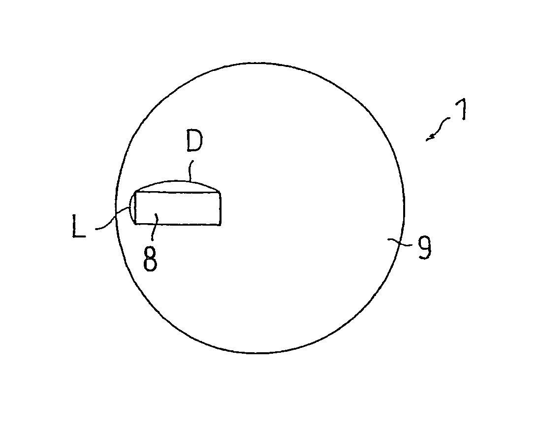
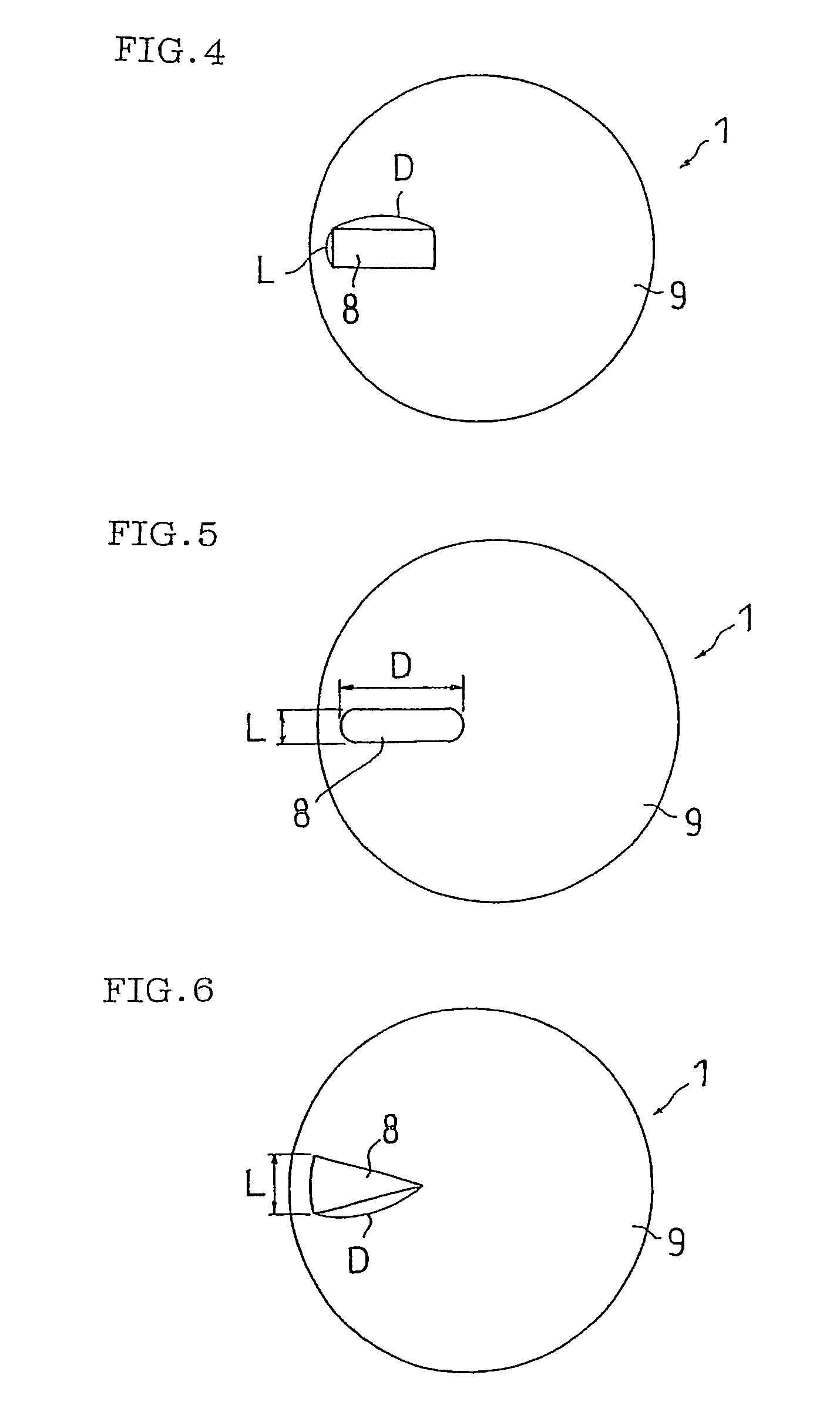
A polishing pad enabling a highly precise optical endpoint sensing during the polishing process and thus having excellent polishing characteristics (such as surface uniformity and in-plane uniformity) is disclosed. A polishing pad enabling to obtain the polishing profile of a large area of a wafer is also disclosed. A polishing pad of a first invention comprises a light-transmitting region having a transmittance of not less than 50% over the wavelength range of 400 to 700 nm. A polishing pad of a second invention comprises a light-transmitting region having a thickness of 0.5 to 4 mm and a transmittance of not less than 80% over the wavelength range of 600 to 700 nm. A polishing pad of a third invention comprises a light-transmitting region arranged between the central portion and the peripheral portion of the polishing pad and having a length (D) in the diametrical direction which is three times or more longer than the length (L) in the circumferential direction.

Description

[0001]This application is the U.S. National Phase under 35 U.S.C. §371 of International Application PCT / JP2003 / .015128, filed Nov. 27, 2003, which claims priority to Japanese Patent Application No. 2002-343199, filed Nov. 27, 2002, No. 2003-000331, filed Jan. 6, 2003, No. 2003-029477, filed Feb. 6, 2003, and No. 2003-064653, filed Mar. 11, 2003. The International Application was not published under PCT Article 21(2) in English.TECHNICAL FIELD[0002]The present invention relates to a polishing pad used in planarizing an uneven surface of a wafer by chemical mechanical polishing (CMP) and in particular to a polishing pad having a window for sensing a polished state etc. by an optical means, as well as a method of producing a semiconductor device by the polishing pad.BACKGROUND ART[0003]Production of a semiconductor device involves a step of forming an electroconductive film on the surface of a wafer to form a wiring layer by photolithography, etching etc., a step of forming an interlam...

Claims


Application Information

Patent Timeline
Patent Type & Authority Patents(United States)
IPC IPC(8): C23F1/00B24B37/013B24B37/20B24B49/12B24D13/14
CPCB24B37/205B24B37/013H01L21/304
Inventor NAKAMORI, MASAHIKOSHIMOMURA, TETSUOYAMADA, TAKATOSHIOGAWA, KAZUYUKIKAZUNO, ATSUSHIWATANABE, MASAHIRO
Owner ROHM & HAAS ELECTRONICS MATERIALS CMP HLDG INC
Learn More