Semiconductor light source apparatus

a technology of semiconductors and light sources, applied in the direction of lighting and heating apparatus, lighting applications, instruments, etc., can solve the problems of difficult for the conventional apparatus b>90/b> to improve the light-emitting density, and the conventional apparatus b>90/b> can achieve the effect of high light-emitting efficiency

Inactive Publication Date: 2014-10-07
STANLEY ELECTRIC CO LTD
View PDF11 Cites 135 Cited by
  • Summary
  • Abstract
  • Description
  • Claims
  • Application Information

AI Technical Summary

Benefits of technology

[0026]In the above-described exemplary light source apparatus, each of the top edge and the bottom edge of the phosphor layer can be formed in a substantially same shape having a central point, and the outer surface of the phosphor layer can be substantially parallel to a central axis connecting the central point of the top edge to the central point of the bottom edge of the phosphor layer in order to enhance a light-emitting density. In addition, each of the top edge and the bottom edge of the phosphor layer can also be formed in a substantially similarity shape having a central point, and the similarity shape shrinks from the bottom edge of the phosphor layer toward the top edge of the phosphor lay along a central axis connecting the central point of the top edge to the central point of the bottom edge of the phosphor layer in order to further enhance a light-emitting density.
[0028]According to the above-described exemplary semiconductor light source apparatuses, the laser light entering into the cavity can repeat reflections on the inner surface of the phosphor layer many a time, each and every time most of the laser light can enter into the phosphor layer having the above-described structures. The laser light can be wavelength converted in the phosphor layer and a focused wavelength converted light can be emitted from a small light-emitting surface. Therefore, the disclosed subject matter can include providing a semiconductor light source apparatus having a high light-emitting efficiency and a high light-emitting density. The semiconductor light source apparatus can emit a substantially natural light having a high light-emitting density such that can be used as a light source for a vehicle headlight and the like, and which can improve a light-emitting efficiency by preventing a back-reflection toward the laser diode.
[0031]According to the above-described exemplary semiconductor light source apparatus, when the laser light gets to the concave surface, most of the laser light can enter into the phosphor layer while being refracted on the concave surface. In this case, a laser light not entering into the phosphor layer can be diffused on the concave surface, and most of the laser light can also enter into the phosphor layer that is formed in a relatively small shape due to diffusing lights. Thus, the disclosed subject matter can include providing semiconductor light source apparatuses having a high light-emitting efficiency, which can improve a light-emitting efficiency by promoting effective use of the back-reflection of the laser light.
[0034]According to another aspect of the disclosed subject matter, the semiconductor light source apparatus can provide various light distributions using the above-described various color lights in accordance with an outer shape of the light-emitting surface exposed from the clad layer and a surface shape of the light-emitting surface, which can be formed using at least one of the planar surface, the convex surface and the concave surface. Thus, the disclosed subject matter can also provide semiconductor light source apparatuses having a high light-emitting efficiency, which can provide various light distribution patterns such as a wide range, a radial fashion and the like, and which can be used for various lighting units such as general lighting, a street light, a stage light, etc., as well as for vehicle lighting applications.

Problems solved by technology

However, it may be difficult for the conventional apparatus 90 to efficiently use the laser light to excite the phosphor 94 because the laser light may be subject to a back-reflection under the phosphor 94.
In addition, it may be difficult for the conventional apparatus 90 to improve a light-emitting density due to a large light-emitting surface, even though the light returning directed toward the reflective board 93 may be repeatedly returned toward the lens 95.
Therefore, the semiconductor light-emitting source apparatus disclosed in Patent Document No. 1 may not be a match for a usage such as a vehicle headlight, in which a light source having a high light-emitting density is desired to provide a light distribution pattern that conforms to a standard for a vehicle headlight.
In addition, because a plurality of light guides 82 may be required to be employed for the above-described usage such as a headlight, a lighting unit using the semiconductor light-emitting source apparatus disclosed in Patent Document No. 1 may become a complex structure in some cases.
Thus, the semiconductor light source apparatus disclosed in Patent Document No. 3 may not also be a match for the above-described usage such as for a headlight, in which a light source having a high light-emitting density is desired to provide a light distribution pattern such that conforms to a standard for a vehicle headlight.

Method used


Image

  • Semiconductor light source apparatus
  • Semiconductor light source apparatus
  • Semiconductor light source apparatus

Examples


first embodiment

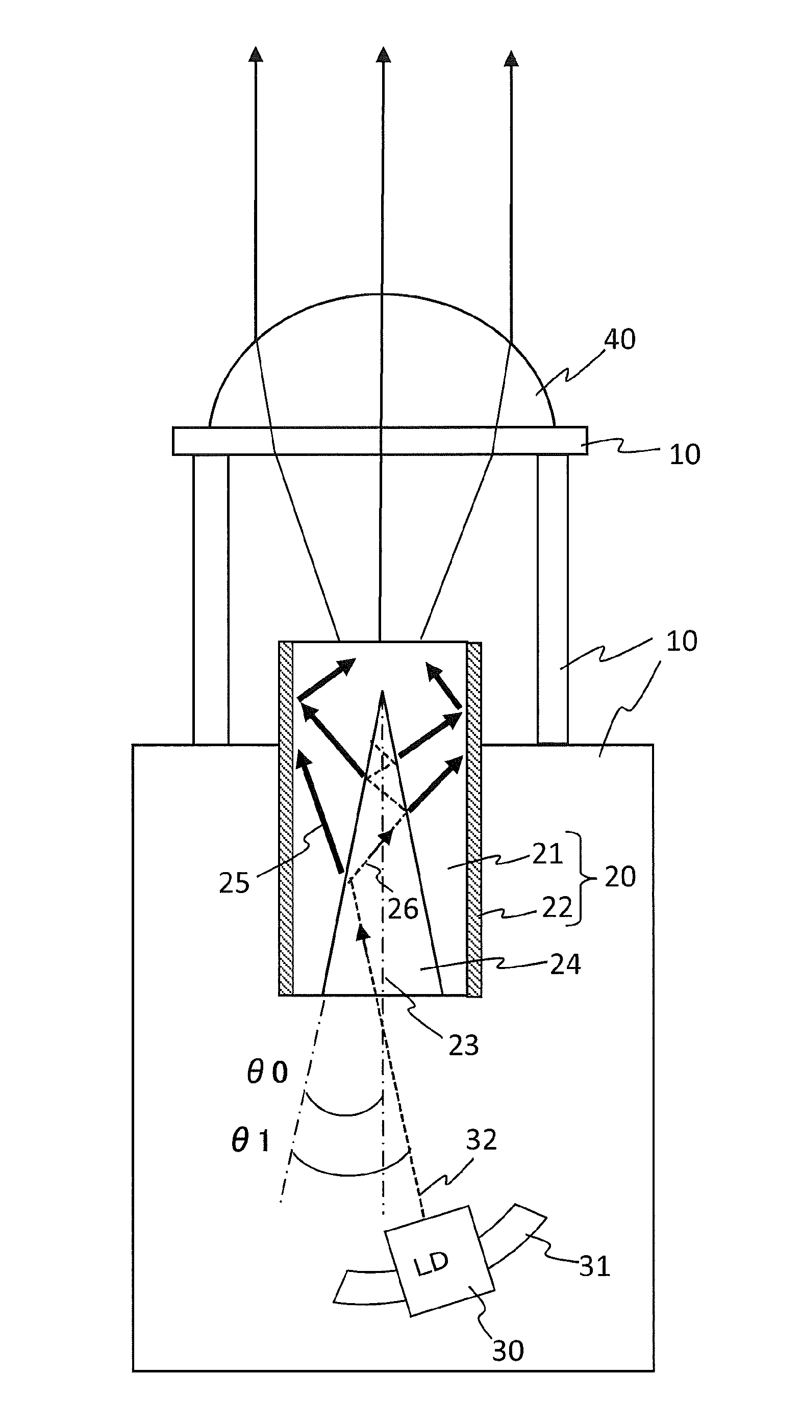
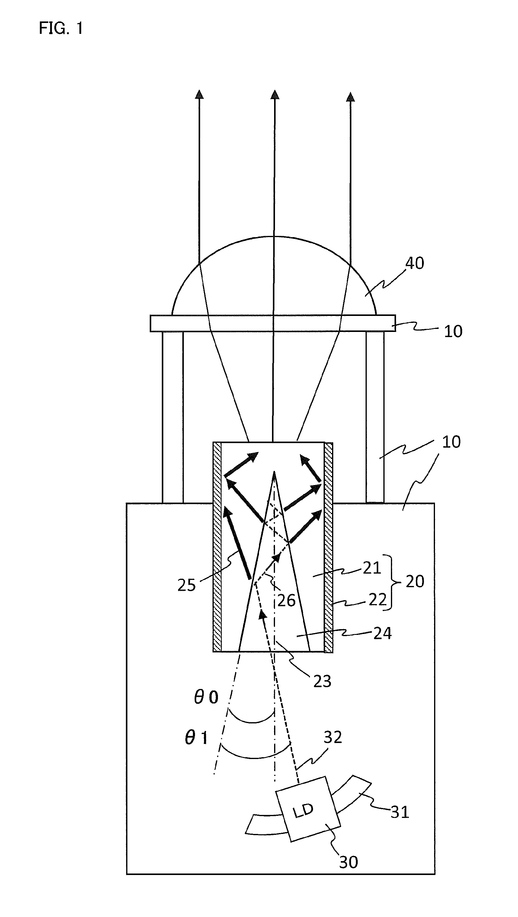
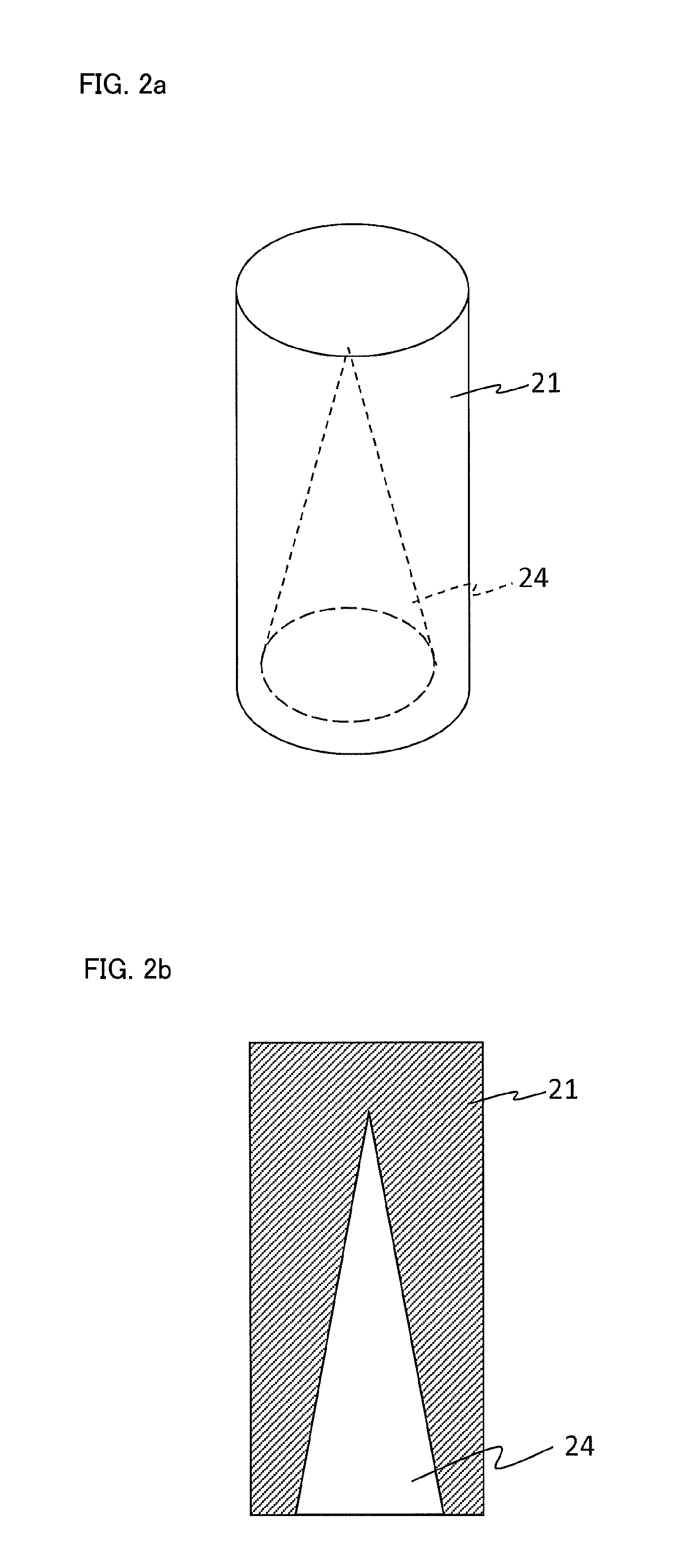
[0063]In the disclosed subject matter, the cavity 24 of the wavelength converting member 20 can be formed in a conical shape, in which the central axis of the circular cone corresponds to the optical axis 23 of the optical lens 40 as described above. An angle of the inner surface of the phosphor layer 21 can be θ0 with respect to the central axis of the cavity 24 as shown in FIG. 1. The angle θ0 of the inner surface of the phosphor layer 21 with respect to the central axis of the cavity 24 will be described in detail later.

[0064]The phosphor layer 21 can be made by dispersing a phosphor powder in a transparent material, and also a glass phosphor that adds a light-emitting ion into a glass and a phosphor ceramic that is composed of a single crystal phosphor or a poly crystal phosphor can be used as the phosphor layer 21, which can wavelength-convert the laser light emitted from the LD 30 into light having a prescribed wavelength. The transparent material in which the phosphor powder ...

third embodiment

[0099]Consequently, even when the incident angle θn of the laser light becomes more than 90 degrees, because the reflective light can be returned in a direction of the inner surface of the phosphor layer 221, the number of the reflections can increase. Thus, the semiconductor light source apparatus of the third embodiment can also improve a light-emitting efficiency because an amount of the laser light entering into the phosphor layer 221 can increase.

[0100]FIG. 8 is a cross-sectional structural view showing a wavelength converting member and moving directions of light rays of a fourth exemplary embodiment of a semiconductor light source apparatus. A difference between the fourth embodiment and the third embodiment of the semiconductor light source apparatus relates to a phosphor layer 321 of the wavelength converting member 320, in which a clad layer 322 is basically the same as the clad layer 222 of the third embodiment.

[0101]A cavity 324 that can form an inner surface of the phos...

fourth embodiment

[0102]Therefore, in the wavelength converting member 320 of the fourth embodiment, the laser light having an incident angle θ1 can enter into the cavity 324 from a part of the opening of the cavity 324 that is not covered with the clad layer 322, and most of the laser light can enter into the phosphor layer 321. A laser light that cannot enter into the phosphor layer 321 may repeat reflections on the inner surface of the phosphor layer 321 many times. Whenever the laser light is reflected on the inner surface of the phosphor layer 321, most of the laser light can enter into the phosphor layer 321.

[0103]When the incident angle θn of the laser light becomes more than 90 degrees, the reflective light may return toward the opening of the cavity 324. However, the reflective light may get to the inner surface of the phosphor layer 321 again after it is reflected on an inner surface of the clad layer 322. Then, a reflective light not entering into the phosphor layer 321 can very often repe...


PUM


Abstract

A semiconductor light source apparatus can include a clad layer, a phosphor layer surrounded by the clad layer and a laser diode emitting a laser light. The phosphor layer can include a cavity having an opening for receiving the laser light, a phosphor material and a light-emitting surface of the apparatus. The laser light entering into the cavity can repeatedly reflect on an inner surface of the phosphor layer many times, each and every time most of the laser light entering into the phosphor layer. The laser light can be efficiently wavelength-converted by the phosphor material and the wavelength converted light can be emitted from the light-emitting surface having various shapes exposed from the clad layer. Therefore, the disclosed subject matter can include providing semiconductor light source apparatuses having a high light-emitting efficiency and high light-emitting density such that the devices can be used for a headlight, general lighting, etc.

Description

[0001]This application claims the priority benefit under 35 U.S.C. §119 of Japanese Patent Application No. 2011-049362 filed on Mar. 7, 2011, which is hereby incorporated in its entirety by reference.BACKGROUND[0002]1. Field[0003]The presently disclosed subject matter relates to a semiconductor light source apparatus including a phosphor layer for wavelength conversion, and more particularly to a high power semiconductor light source apparatus using a laser light as an excitation light, which can improve a light-emitting efficiency by efficiently combining the laser light into the phosphor layer, and which can also emit various color lights including a natural light having a large amount of light intensity in order to be able to be used for a laser headlight, general lighting, a stage light, a street light, etc.[0004]2. Description of the Related Art[0005]Semiconductor light source apparatuses that emit various color lights including white light by combining a phosphor with a semico...

Claims


Application Information

Patent Timeline
Patent Type & Authority Patents(United States)
IPC IPC(8): F21V9/16F21S8/10F21W131/103F21W131/406F21Y101/02
CPCF21V9/16F21S48/1145F21W2131/103F21Y2101/025F21W2131/406F21V13/14F21Y2115/10F21Y2115/30F21S41/16F21S41/176F21V9/32
Inventor HARADA, MITSUNORI
Owner STANLEY ELECTRIC CO LTD
Why Eureka
Try Eureka