
Semiconductor memory device

a memory device and semiconductor technology, applied in the direction of solid-state devices, transistors, instruments, etc., can solve the problems of difficult to realize a multi-level memory cell in consideration of reading margin, and achieve the effect of increasing the storage capacity of the memory module per unit area

Inactive Publication Date: 2014-10-07
SEMICON ENERGY LAB CO LTD
View PDF132 Cites 20 Cited by
  • Summary
  • Abstract
  • Description
  • Claims
  • Application Information

AI Technical Summary

Benefits of technology

[0016]Further, it is another object of one embodiment of the present invention to provide a memory module with small power consumption.
[0030]Further, the frequency of a refresh operation in a memory cell is reduced, and thereby the power consumption of a memory module can be reduced.

Problems solved by technology

However, it is difficult to realize a multilevel memory cell in consideration of margin of reading.

Method used


Image

  • Semiconductor memory device
  • Semiconductor memory device
  • Semiconductor memory device

Examples


embodiment 1

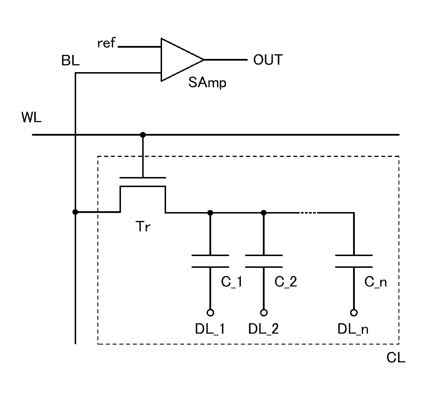
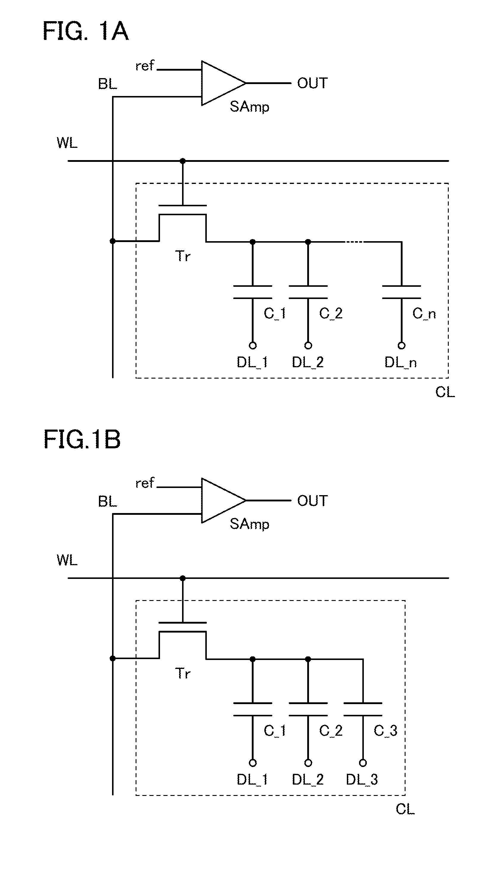
[0046]In this embodiment, examples of a structure and an operation of a memory cell that is one of semiconductor memory devices will be described with reference to FIGS. 1A and 1B.

[0047]FIG. 1A is a circuit diagram illustrating a 2n-level memory cell which includes a bit line BL; a word line WL; data lines DL_1 to DL_n; a memory cell CL having a transistor Tr and capacitors C_1 to C_n; and a sense amplifier SAmp.

[0048]A gate of the transistor Tr is connected to the word line WL, one of a source and a drain of the transistor Tr is connected to the bit line BL, the other thereof is connected to one side of each of the capacitors C_1 to C_n, and the other sides of the capacitors C_1 to C_n are connected to the data lines DL_1 to DL_n. For example, the capacitor C_1, the capacitor C_2, and the capacitor C_n are connected to the data line DL_1, the data line DL_2, and the data line DL_n, respectively. The bit line BL is connected to the sense amplifier SAmp.

[0049]As the transistor Tr, a ...

embodiment 2

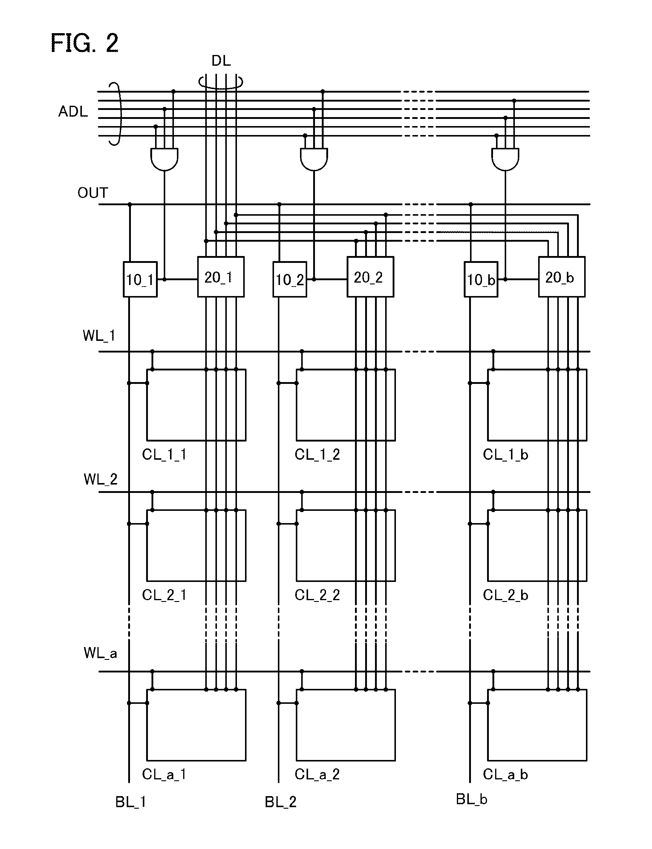
[0068]In this embodiment, a memory module having a rows and b columns using the memory cells described in Embodiment 1 will be described with reference to FIG. 2, as one example of semiconductor memory devices.

[0069]FIG. 2 illustrates a memory module including an address line ADL, a data line DL, bit lines BL_1 to BL_b, word lines WL_1 to WL_a, AND circuits, an output OUT, reading circuits 10_1 to 10—b, switching circuits 20_1 to 20—b, and memory cells CL_1_1 to CL_a_b.

[0070]The address lines ADL are connected to the reading circuits 10_1 to 10—b and the switch circuits 20_1 to 20—b via AND circuits. The data lines DL are each connected to a corresponding capacitor in the memory cells CL_1_1 to CL_a_b via the switch circuits 20_1 to 20—b. The bit line BL_1 is connected to one of a source and a drain of a transistor in each of the memory cells CL_1_1 to CL_a_1 and to the output OUT via the reading circuit 10_1. Similarly, the bit line BL_2 and BL_b are connected to one of a source an...

embodiment 3

[0085]In this embodiment, a memory cell that is one of semiconductor memory devices will be described with reference to FIGS. 3A and 3B.

[0086]FIG. 3A is a cross-sectional view of a semiconductor memory device including a region 300 having a semiconductor substrate 331 and a first insulating film 332; a second insulating film 302 over the region 300; an island-shaped semiconductor film 306 provided over the second insulating film 302; a conductive film 308 and a conductive film 309 which are partially in contact with the semiconductor film 306; a third insulating film 312 provided over the semiconductor film 306, the conductive film 308, and the conductive film 309; a conductive film 304 overlapped with the semiconductor film 306 with the third insulating film 312 interposed therebetween; conductive films 341 to 344 formed with the same layer as the conductive film 304; and a fourth insulating film 316 provided to cover the third insulating film 312, the conductive film 304, and the ...


PUM


Abstract

To increase a storage capacity of a memory module per unit area, and to provide a memory module with low power consumption, a transistor formed using an oxide semiconductor film, a silicon carbide film, a gallium nitride film, or the like, which is highly purified and has a wide band gap of 2.5 eV or higher is used for a DRAM, so that a retention period of potentials in a capacitor can be extended. Further, a memory cell has n capacitors with different capacitances and the n capacitors are each connected to a corresponding one of n data lines, so that a variety of the storage capacitances can be obtained and multilevel data can be stored. The capacitors may be stacked for reducing the area of the memory cell.

Description

BACKGROUND OF THE INVENTION[0001]1. Field of the Invention[0002]The present invention relates to semiconductor memory devices.[0003]2. Description of the Related Art[0004]A dynamic random access memory (DRAM) is a semiconductor memory device where one bit of data can be stored with use of one transistor and one capacitor. The DRAM has a small area per memory cell, easiness in integration for modularization, and is manufactured at low cost.[0005]In a DRAM, electric charges stored in a capacitor are leaked due to off-state current of a transistor, and thus an operation of recharge (refresh) is required before charges are lost.REFERENCE[0006][Patent Document 1] Japanese Published Patent Application No. H6-295589SUMMARY OF THE INVENTION[0007]A DRAM will be explained with reference to a circuit diagram of FIG. 8A. A DRAM includes a bit line BL, a word line WL, a sense amplifier SAmp, a transistor Tr, and a capacitor C.[0008]It is known that the potential stored in the capacitor is reduce...

Claims


Application Information

Patent Timeline
Patent Type & Authority Patents(United States)
IPC IPC(8): G11C11/24G11C11/404H01L21/84H01L27/108H01L27/12H01L49/02
CPCG11C11/404H01L28/60H01L27/108H01L27/1203H01L21/84H01L28/40H01L27/10873H01L27/1085H01L27/10852G11C11/401H10B12/00H10B12/03H10B12/033H10B12/05G11C11/4097H10B12/30H10B12/33G11C11/4096H01L29/7869
Inventor SAITO, TOSHIHIKO
Owner SEMICON ENERGY LAB CO LTD
Learn More