Transistor, method of manufacturing the transistor, semiconductor unit, method of manufacturing the semiconductor unit, display, and electronic apparatus

a technology of transistors and semiconductors, applied in the field of transistors, can solve problems such as image quality degradation, and achieve the effect of improving electrical characteristics

Active Publication Date: 2014-11-11
JOLED INC
View PDF8 Cites 4 Cited by
  • Summary
  • Abstract
  • Description
  • Claims
  • Application Information

AI Technical Summary

Benefits of technology

[0006]In the above-described transistor using the oxide semiconductor film, desirably, the oxide semiconducto...

Problems solved by technology

However, if a parasitic capacity generated in a cross region between the gate electrode and the source-drain elect...

Method used


Image

  • Transistor, method of manufacturing the transistor, semiconductor unit, method of manufacturing the semiconductor unit, display, and electronic apparatus
  • Transistor, method of manufacturing the transistor, semiconductor unit, method of manufacturing the semiconductor unit, display, and electronic apparatus
  • Transistor, method of manufacturing the transistor, semiconductor unit, method of manufacturing the semiconductor unit, display, and electronic apparatus

Examples


first embodiment (

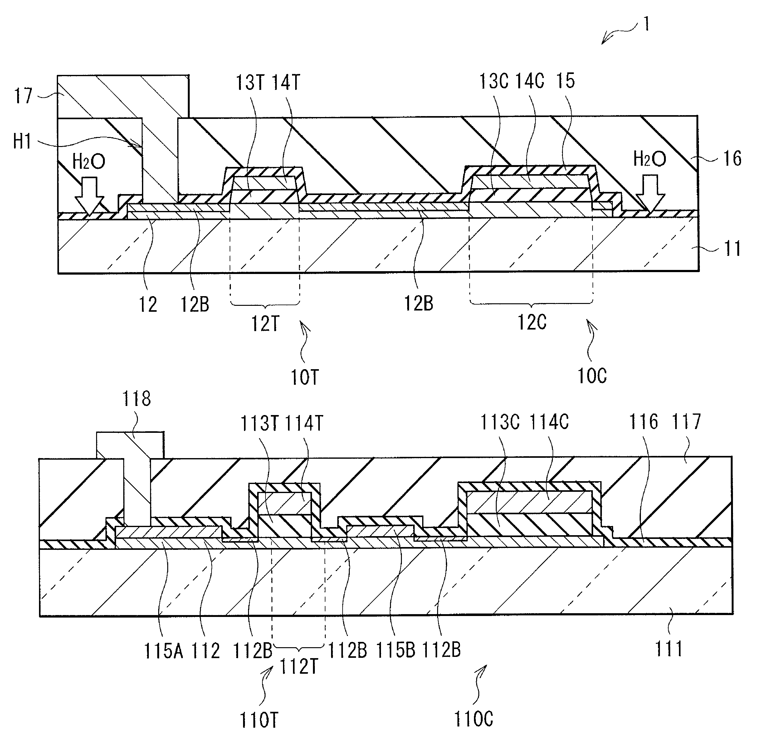
1. First Embodiment (an example of an organic EL display in which a substrate is formed of only a plate-like member)

2. Modification 1 (an example of a liquid crystal display)

3. Modification 2 (an example of an electronic paper)

second embodiment (

4. Second Embodiment (an example in which a substrate having a diffusion preventing film)

third embodiment (

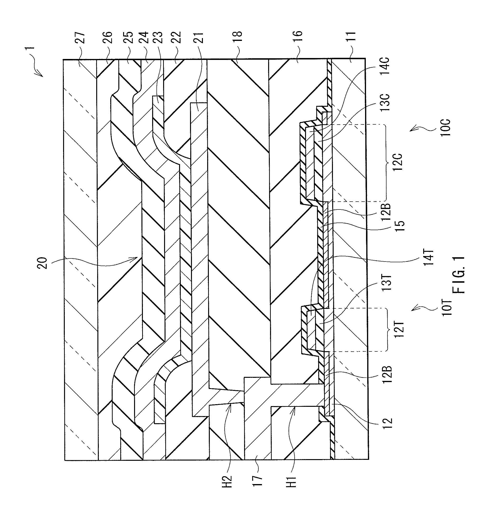
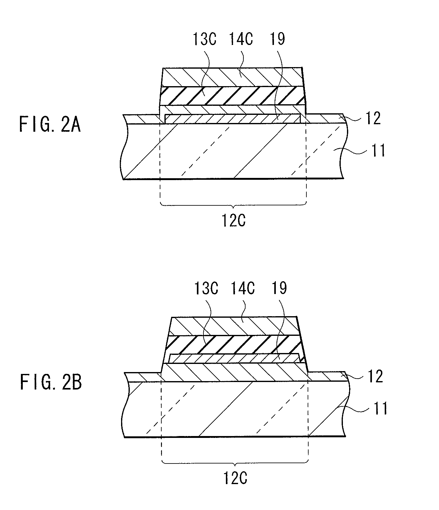
5. Third Embodiment (an organic EL display: an example in which a channel protection film is provided between an oxide semiconductor film and an oxide film)

6. Modification 3 (an example in which a side surface of an oxide semiconductor film and a side surface of a channel protection film are aligned)

7. Modification 4 (an example in which a wiring connecting an oxide semiconductor film and one of electrodes of a retention capacitor is provided)


PUM


Abstract

A method of manufacturing a transistor includes: forming an oxide semiconductor film and a gate electrode on a substrate, the oxide semiconductor film having a channel region, and the gate electrode facing the channel region; and forming an insulating film covering the gate electrode and the oxide semiconductor film. Infiltration of moisture from the insulating film into the oxide semiconductor film is suppressed by the substrate.

Description

CROSS REFERENCES TO RELATED APPLICATIONS[0001]The present application claims priority to Japanese Priority Patent Application JP 2012-041561 filed in the Japan Patent Office on Feb. 28, 2012, and 2012-047586 filed in the Japan Patent Office on Mar. 5, 2012, the entire content of which is hereby incorporated by reference.BACKGROUND[0002]The present application relates to a transistor using an oxide semiconductor, a method of manufacturing the transistor, a semiconductor unit, a method of manufacturing the semiconductor unit, and to a display and an electronic apparatus which are provided with the transistor.[0003]In recent years, along with increase in size and definition of a display, a thin film transistor (TFT) of a drive device is also demanded to have a high mobility, and a TFT using an oxide semiconductor such as oxide of zinc (Zn), indium (In), gallium (Ga), tin (Sn), aluminum (Al), or titanium (Ti), or an oxide of a mixture thereof has been developed. In particular, a TFT usi...

Claims


Application Information

Patent Timeline
IPC IPC(8): H01L21/84H01L29/786H01L21/00H01L27/12H01L29/66
CPCH01L27/1255H01L29/66742H01L27/1225H01L29/786H01L29/7869H01L29/78606H01L27/1248H01L29/78693H01L21/324
Inventor MOROSAWA, NARIHIROTOYOTA, MOTOHIRO
Owner JOLED INC
Why Eureka
Try Eureka