

Light-emitting element, light-emitting device, display device, and electronic apparatus
a technology of light-emitting devices and light-emitting elements, which is applied in the direction of solid-state devices, semiconductor devices, thermoelectric devices, etc., can solve the problems of degrading the ability of the hole transport layer to block electrons, the layer cannot sufficiently block electrons, and the problem of increasing the problem of amplification
- Summary
- Abstract
- Description
- Claims
- Application Information
AI Technical Summary
Benefits of technology
Problems solved by technology
Method used
Image

Examples
example 1
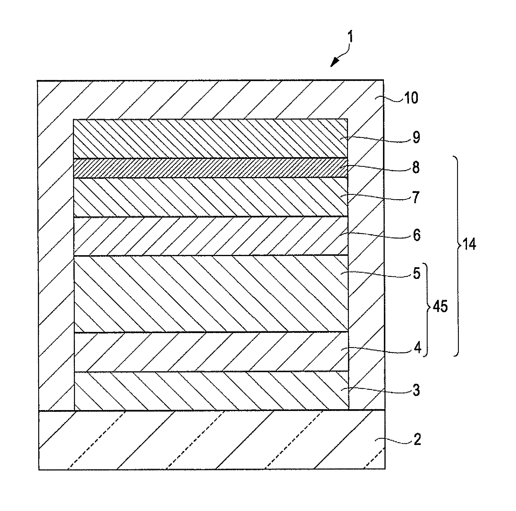
[0178](1) First, a transparent glass substrate having an average thickness of 0.5 mm was prepared. Then, an ITO electrode (anode) was formed to an average thickness of 150 nm on the substrate by sputtering. After being subjected to ultrasonic cleaning in acetone and 2-propanol in that order, the resulting substrate was treated with oxygen plasma and argon plasma. The treatments with these plasmas were each performed at a plasma power of 100 W and a gas flow rate of 20 sccm for 5 seconds with the substrate heated to 70 to 90° C.
[0179](2) Subsequently, a hole injection layer having an average thickness of 20 nm was formed on the ITO electrode by vacuum vapor codeposition of the benzidine derivative (hole injection material) expressed by formula (1) and the anthracene derivative (electron transport material) expressed by the following formula (10). In this Example, the hole injection layer was made of a mixture of the benzidine derivative (hole injection material) expressed by formula ...
example 2
[0188]A light-emitting element was produced in the same manner as in Example 1 except that the weight ratio of the benzidine derivative to the anthracene derivative in the hole injection layer was set to 30:70.
example 3
[0189]A light-emitting element was produced in the same manner as in Example 1 except that the weight ratio of the benzidine derivative to the anthracene derivative in the hole injection layer was set to 50:50.
PUM
 Abstract
Description
Claims
Application Information