Compliant printed circuit socket diagnostic tool

a diagnostic tool and printed circuit technology, applied in continuity testing, instruments, measurement devices, etc., can solve the problems of taking weeks to generate a revision, traditional methods, etc., and achieve the effects of simple low-cost, high-performance interconnection, and increased value for users

Inactive Publication Date: 2015-01-06
HSIO TECH
View PDF358 Cites 40 Cited by
  • Summary
  • Abstract
  • Description
  • Claims
  • Application Information

AI Technical Summary

Benefits of technology

[0011]The present disclosure aims to leverage the capabilities of printed electronics to provide a diagnostic tool to validate socket function either external to the system or while the socket is installed in the system. The present disclosure provides an electrical interconnect that can enable next generation electrical performance. Some of the embodiments include a high performance interconnect architecture on the interconnect.
[0012]Printing processes permit compliant printed circuits and electrical devices of diagnostic tools to be produced by a direct writing method based upon images, without the need for artwork, lengthy lead-times for circuit design and production, and subtractive circuit techniques. The present diagnostic tools can be simple or complex, and can be produced in minutes. The diagnostic tools can also be adapted as needed to accommodate additional diagnostic functions or tests. The additive nature of many printing processes, such as for example the inkjet printing process, can also provide an excellent avenue to directly print electrical devices as part of printing the diagnostic tools. The electrical devices that may be printed may include, but are not limited to, passive components, transistors, display function or adaptive intelligence. Revisions to the diagnostic tools can be accomplished in moments by altering the image files and reprinting the diagnostic tools. Traditional methods, by contrast, may take weeks to generate a revision.
[0013]A diagnostic tool can be as simple as a daisy chain to verify continuity, or as complex as functional testing directly on the diagnostic tool. Positioning functional testing on the present diagnostic tool dramatically increases the value to the user by eliminating a need to connect to external systems or testing analyzers. The diagnostic tools can be printed with simple low-cost or low-speed circuitry, or the circuitry can be printed with high frequency capability in the event an external measurement tool is connected.
[0014]The cost to produce a diagnostic tool in accordance with the present disclosure is a fraction the of cost of a conventional tool. A tool produced with conventional methods might cost $10,000 to $20,000 to design and produce, typically with a 4-6 week lead-time. A diagnostic tool according to the present disclosure can be produced in minutes for a fraction of the cost. The ability to modify the design or correct errors which would cause the $20,000 investment to be wasted, and reprint and reprint the tool easily at little additional cost, offers tremendous improvements over conventional methods. Image libraries and design rules can be created to semi-automate the design process and dramatically reduce engineering time, with tremendous flexibility to make changes substantially on the fly during the testing process.
[0015]The use of additive printing processes can permit the material set in a given layer to vary. Traditional PCB and circuit fabrication methods take sheets of material and stack them up, laminate, and / or drill. The materials in each layer are limited to the materials in a particular sheet. Additive printing technologies permit a wide variety of materials to be applied on a layer with a registration relative to the features of the previous layer. Selective addition of conductive, non-conductive, or semi-conductive materials at precise locations to create a desired effect has the major advantages in tuning impedance or adding electrical function on a given layer. Tuning performance on a layer by layer basis relative to the previous layer greatly enhances electrical performance.
[0016]The compliant printed circuit can also be processed to add functions and electrical enhancements not found in traditional printed circuits. The diagnostic tool according to the present disclosure can be configured with conductive traces that reduce or redistribute the terminal pitch, without the addition of an interposer or daughter substrate. Grounding schemes, shielding, electrical devices, and power planes can be added to the present diagnostic tools, reducing the number of connections to the PCB and relieving routing constraints while increasing performance.

Problems solved by technology

Traditional methods, by contrast, may take weeks to generate a revision.

Method used


Image

  • Compliant printed circuit socket diagnostic tool
  • Compliant printed circuit socket diagnostic tool
  • Compliant printed circuit socket diagnostic tool

Examples


Embodiment Construction

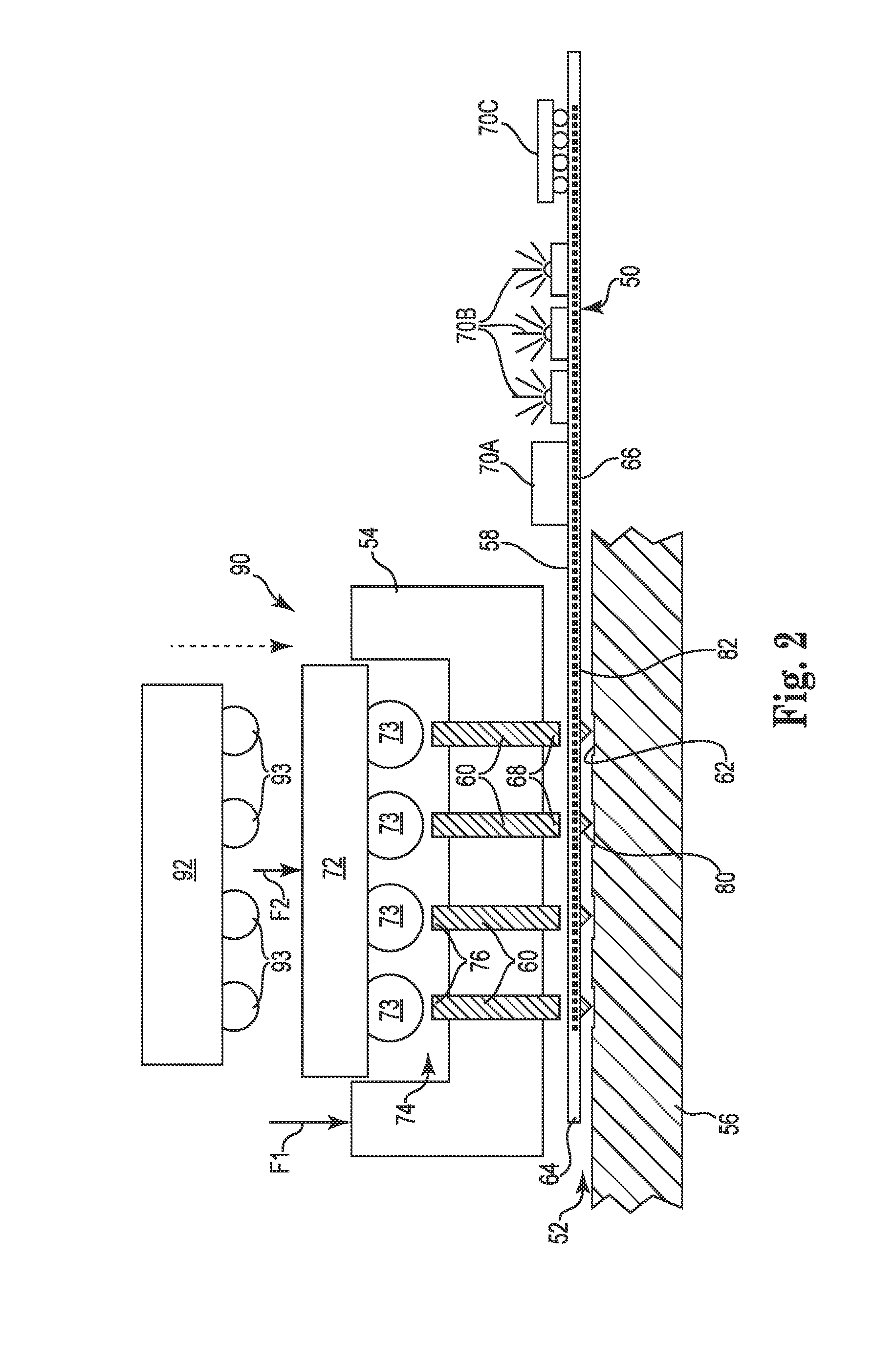
[0033]FIG. 2 is a schematic illustration of a diagnostic tool 50 electrically coupled at an interface 52 of a socket 54 and a printed circuit board (PCB) 56 in accordance with an embodiment of the present disclosure. A compliant printed circuit 58 of the diagnostic tool 50 is positioned to act as an electrical interconnect between contact members 60 on the socket 54 and contact pads 62 on the PCB 56.

[0034]The present compliant printed circuit 58 can operate with fine contact-to-contact spacing (pitch) on the order of less than 1.0 millimeter, and more preferably a pitch of less than about 0.7 millimeter, and most preferably a pitch of less than about 0.4 millimeter. The socket 54 permits IC packages 72, 92 to be installed and uninstalled without the need to reflow solder.

[0035]The compliant printed circuit 58 is a flexible polymeric sheet 64 with a plurality of conductive traces 66 arranged in an array to electrically couple with proximal ends 68 of the contact members 60 and contac...


PUM

PropertyMeasurementUnit
lead-timeaaaaaaaaaa
aspect ratioaaaaaaaaaa
widthaaaaaaaaaa

Abstract

Diagnostic tools for testing integrated circuit (IC) devices, and a method of making the same. The first diagnostic tool includes a first compliant printed circuit with a plurality of contact pads configured to form an electrical interconnect at a first interface between proximal ends of contact members in the socket and contact pads on a printed circuit board (PCB). A plurality of printed conductive traces electrically couple to a plurality of the contact pads on the first compliant printed circuit. A plurality of electrical devices are printed on the first compliant printed circuit at a location external to the first interface. The electrical devices are electrically coupled to the conductive traces and programmed to provide one or more of continuity testing at the first interface or functionality of the IC devices. A second diagnostic tool includes a second compliant printed circuit electrically coupled to a surrogate IC device.

Description

CROSS-REFERENCE TO RELATED APPLICATIONS[0001]This application is a national stage application under 35 U.S.C. §371 of International Application No. PCT / US2010 / 036377, titled COMPLIANT PRINTED CIRCUIT SOCKET DIAGNOSTIC TOOL, filed May 27, 2010, which claims priority to U.S. Provisional Application No. 61 / 183,397, filed Jun. 2, 2009, both of which are hereby incorporated by reference in their entireties.FIELD OF THE INVENTION[0002]The present application relates to a compliant printed circuit that provides an electrical interconnect with integrated circuit devices, sockets and printed circuits, and in particular, to a diagnostic tool for testing IC devices, sockets, and printed circuit boards.BACKGROUND OF THE INVENTION[0003]There are many applications where a socket is used to connect an integrated circuit (IC) device to a printed circuit board (PCB) so that the electrical connection is made in a separable manner. As illustrated in FIG. 1, a socket 20 in a test system 21 may receive ...

Claims


Application Information

Patent Timeline
Patent Type & Authority Patents(United States)
IPC IPC(8): G01R31/00G01R31/02G01R31/28
CPCG01R31/2889G01R31/024G01R31/54Y10T29/49004
Inventor RATHBURN, JAMES
Owner HSIO TECH
Why Eureka
Try Eureka