Conformal doping via plasma activated atomic layer deposition and conformal film deposition

a technology of conformal film and atomic layer, which is applied in the direction of coating, chemical vapor deposition coating, semiconductor devices, etc., can solve the problems of difficult doping, difficulty in doping sidewalls, and vertical structures

Active Publication Date: 2015-02-17
NOVELLUS SYSTEMS
View PDF225 Cites 446 Cited by
  • Summary
  • Abstract
  • Description
  • Claims
  • Application Information

AI Technical Summary

Problems solved by technology

These vertical structures are difficult to dope using conventional ion implantation techniques, plasma doping techniques, and generally, techniques which involve transport of ions under an electric field.
The difficulty is generally manifest when doping sidewalls, and especially manifest in high aspect ratio structures.
Thus, since ion implantation processes are largely directional, they tend to be incompatible with the fabrication of many gate architecture designs, such as 3D gate designs and / or gate architectures having closely spaced fins which may require doping on lateral and vertical surfaces.
If attempt is made to use ion implantation for doping these surfaces such as by changing the implant tilt angle, this may lead to considerable variability in the dopant dose retention and diffusion range, especially on the sidewalls.
Frequently, in a dense array of i3D structures, there can be shadowing effects for the directional ion beam in an implanter, giving rise to serious dose retention problems for tilted implant angles.
However, there appear to be two primary disadvantages to this technique: (a) it may lead to simultaneous sputter erosion, which may be due to the high energy ions in the plasma, and (b) dopant dose and conformality seem to sensitively depend on the ion to radical density ratio in the plasma, which leads to difficulties in process control.

Method used


Image

  • Conformal doping via plasma activated atomic layer deposition and conformal film deposition
  • Conformal doping via plasma activated atomic layer deposition and conformal film deposition
  • Conformal doping via plasma activated atomic layer deposition and conformal film deposition

Examples


Embodiment Construction

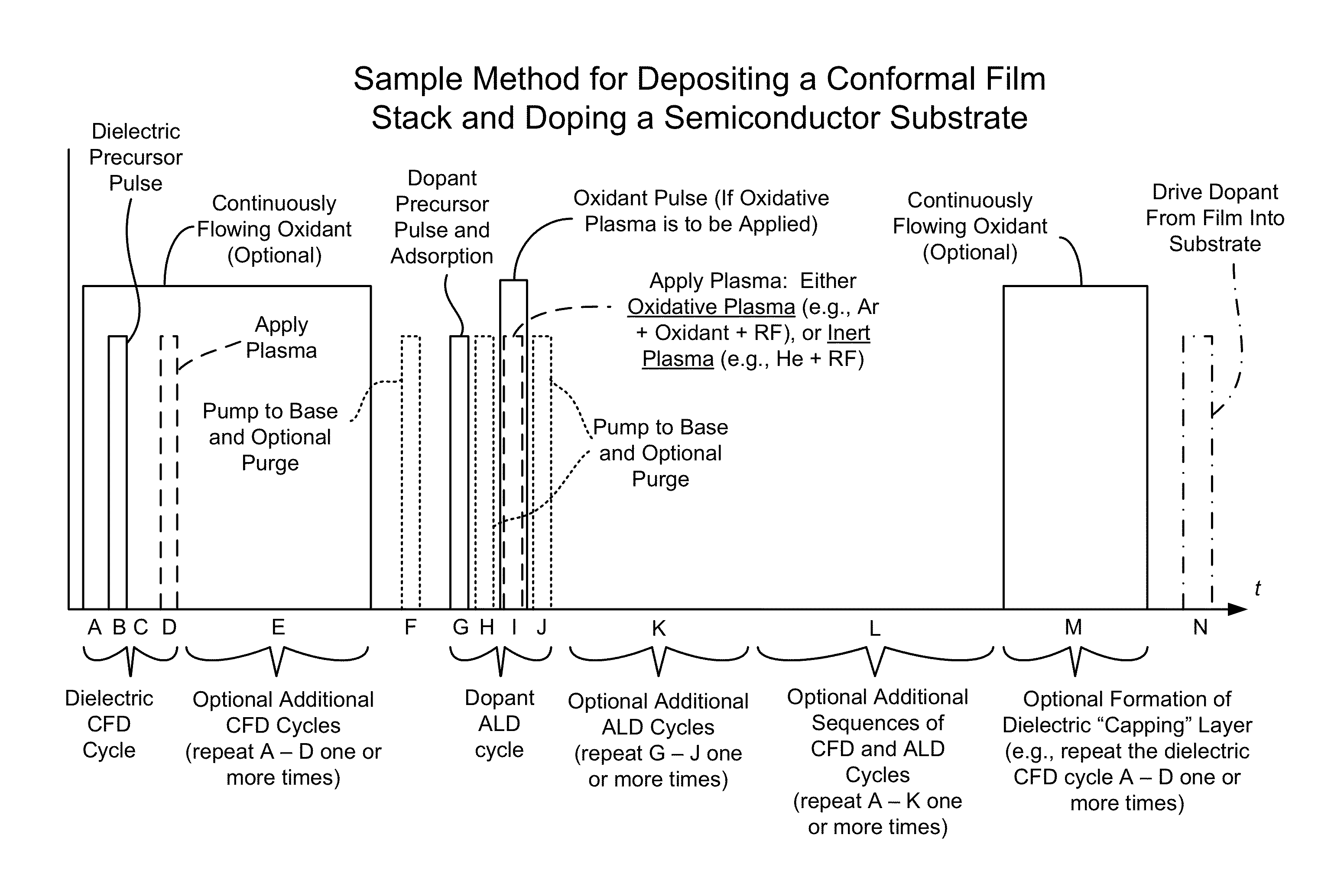
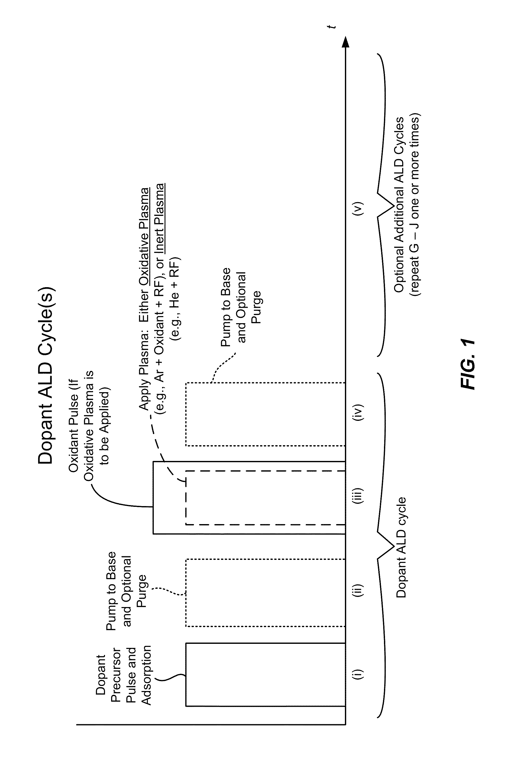
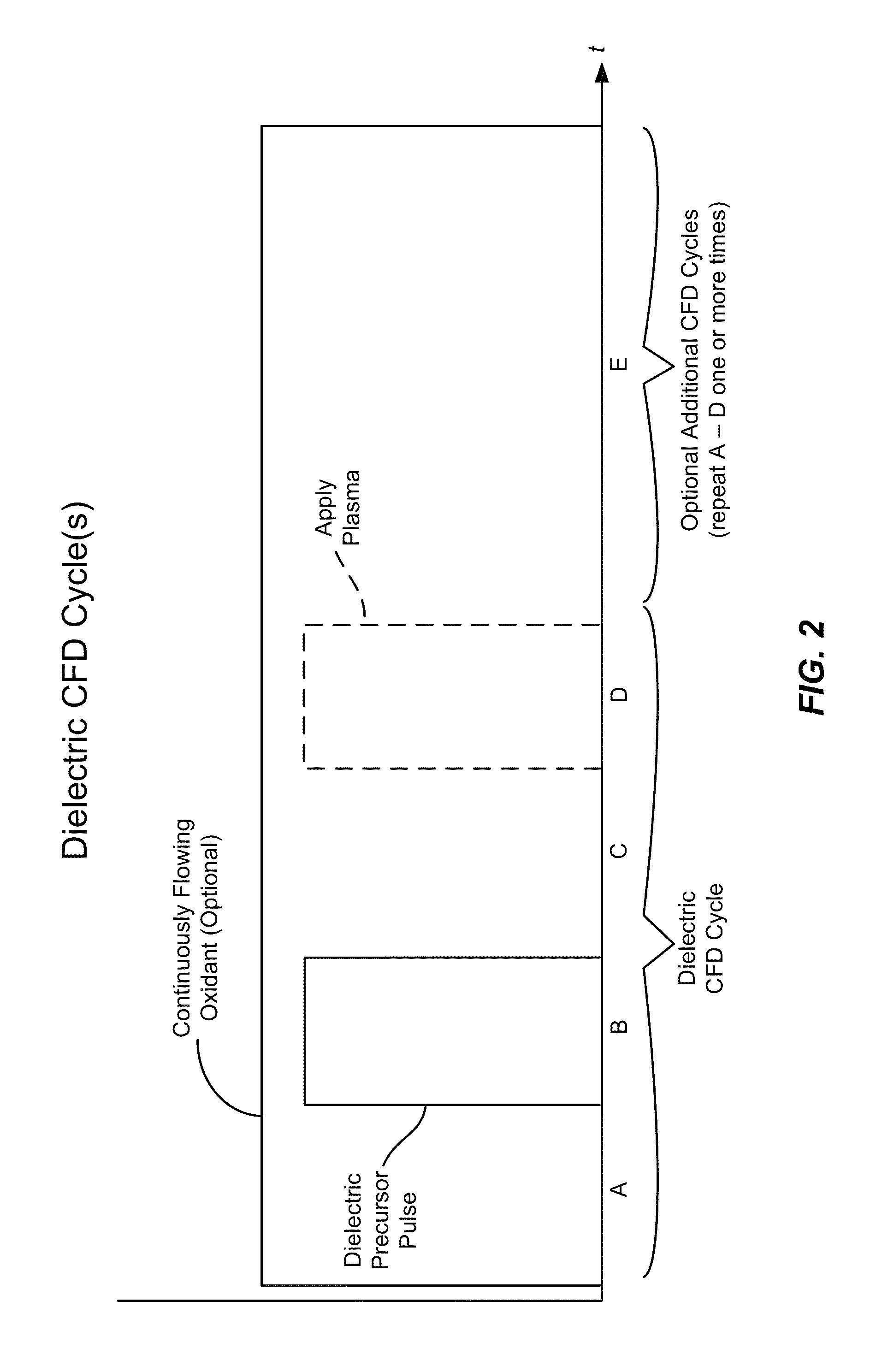
[0033]Solid-state diffusion of p-type and n-type dopants from conformally deposited films are presented herein as an alternative to doping substrates using the incumbent ion implantation technology. Doping via conformally deposited films may be superior to ion implantation when doping, for example, 3D structures such as the ultrashallow junction regions and / or source / drain extension regions of 3D transistors (such as pMOS FinFETs). Generally, doping via conformally deposited films is useful for doping many high aspect ratio devices structures, and may be appropriately used in many scenarios where conventional ion implantation or directional doping methods are inadequate. Such conformal doping may employ the use of deposition techniques such as atomic layer deposition (ALD). In some contexts, a form of ALD referred to as conformal film deposition (CFD) is employed. In particular, when a thin layer of n-doped or p-doped conformal film is formed via ALD over the vertical surfaces of de...


PUM

PropertyMeasurementUnit
thicknessaaaaaaaaaa
thicknessaaaaaaaaaa
widthaaaaaaaaaa

Abstract

Disclosed herein are methods of doping a patterned substrate in a reaction chamber. The methods may include forming a first conformal film layer which has a dopant source including a dopant, and driving some of the dopant into the substrate to form a conformal doping profile. In some embodiments, forming the first film layer may include introducing a dopant precursor into the reaction chamber, adsorbing the dopant precursor under conditions whereby it forms an adsorption-limited layer, and reacting the adsorbed dopant precursor to form the dopant source. Also disclosed herein are apparatuses for doping a substrate which may include a reaction chamber, a gas inlet, and a controller having machine readable code including instructions for operating the gas inlet to introduce dopant precursor into the reaction chamber so that it is adsorbed, and instructions for reacting the adsorbed dopant precursor to form a film layer containing a dopant source.

Description

CROSS REFERENCE TO RELATED APPLICATIONS[0001]This application is a continuation-in-part of, and claims priority to, U.S. patent application Ser. No. 13 / 242,084, filed Sep. 23, 2011, and titled “PLASMA ACTIVATED CONFORMAL DIELECTRIC FILM DEPOSITION.”[0002]U.S. patent application Ser. No. 13 / 242,084 is a continuation-in-part of U.S. patent application Ser. No. 13 / 084,399, filed Apr. 11, 2011, titled “PLASMA ACTIVATED CONFORMAL DIELECTRIC FILM DEPOSITION,” which claims priority to U.S. Provisional Patent Application No. 61 / 324,710, filed Apr. 15, 2010, and U.S. Provisional Patent Application No. 61 / 372,367, filed Aug. 10, 2010, and U.S. Provisional Patent Application No. 61 / 379,081, filed Sep. 1, 2010, and U.S. Provisional Patent Application No. 61 / 417,807, filed Nov. 29, 2010.[0003]U.S. patent application Ser. No. 13 / 242,084 is also a continuation-in-part of U.S. patent application Ser. No. 13 / 084,305, filed Apr. 11, 2011.[0004]This application also claims priority to U.S. Provisional...

Claims


Application Information

Patent Timeline
Patent Type & Authority Patents(United States)
IPC IPC(8): H01L21/469H01L21/31H01L21/311C23C16/04C23C16/34C23C16/40C23C16/455C23C16/56H01L21/02H01L21/225H01L21/768H01L29/66
CPCC23C16/045C23C16/345C23C16/401C23C16/402C23C16/45523C23C16/4554C23C16/56H01L21/02129H01L21/02164H01L21/0217H01L21/022H01L21/02274H01L21/0228H01L21/02348H01L21/76898H01L21/76831C23C16/45531H01L21/2255H01L29/66803
Inventor SWAMINATHAN, SHANKARSRIRAM, MANDYAMVAN SCHRAVENDIJK, BARTSUBRAMONIUM, PRAMODLAVOIE, ADRIEN
Owner NOVELLUS SYSTEMS
Why Eureka
Try Eureka