Laser diode device, method of driving the same, and laser diode apparatus

a laser diode and laser diode technology, applied in the direction of laser details, laser output parameters control, semiconductor lasers, etc., can solve the problems of complex and difficult structure, insufficient light output,

Active Publication Date: 2015-03-24
SONY CORP +1
View PDF32 Cites 0 Cited by
  • Summary
  • Abstract
  • Description
  • Claims
  • Application Information

AI Technical Summary

Benefits of technology

[0008]As described above, regarding an example that a high output is pursued based on “all semiconductor” as an essential requirement for realizing ultimate miniaturization, that is, regarding a laser diode apparatus that does not need mechanical parts or optical parts but is composed of only a laser diode or a combination of a laser diode and a semiconductor device, almost no report exists particularly in a 405 nm band laser diode composed of GaN compound semiconductor. However, if “all semiconductor” pulse laser having a high peak output is able to be realized in 405 nm band, such a pulse laser is able to be used as a light source of a stacked volumetric optical disc system expected as a next generation optical disc system after the Blu-ray optical disc system. In addition, a simple and convenient ultrashort pulse and ultrahigh power light source covering all wavelength bands in the visible light range is able to be realized, and a light source requested in the medical field, the bio imaging field and the like is able to be provided. Further, in the nanoengineered field, it is expected to obtain a highly fine processing equipment.
[0010]Accordingly, in the invention, it is desirable to provide an ultrashort pulse and ultrahigh power laser diode device capable of outputting pulse laser light having higher peak power with a simple composition and a simple structure, a method of driving the same, and a laser diode apparatus mounting such a laser diode device.
[0019]In the laser diode device or the method of driving the same according to the first aspect or the second aspect of the invention or the laser diode apparatus according to the first aspect or the second aspect of the invention, the second compound semiconductor layer is provided with the electron barrier layer having a thickness of 1.5*10−8 m or more. In the laser diode device or the method of driving the same according to the first aspect of the invention and the laser diode apparatus according to the first aspect of the invention, the laser diode device is driven by a pulse current having a value 10 or more times as large as the threshold current value Ith. In the laser diode device or the method of driving the same according to the second aspect of the invention and the laser diode apparatus according to the second aspect of the invention, the laser diode device is driven by a pulse voltage having a value twice or more as large as a threshold voltage value Vth. In result, an ultrashort pulse and ultrahigh power laser diode device that outputs laser light having 70 watt or more peak power was able to be obtained. By combining the laser diode device with a commercially available electric drive electronics, a laser diode apparatus (laser light source) having watt level or more peak light intensity is able to be easily obtained.

Problems solved by technology

Thus, as a light source necessary for a high peak output used for, for example, two-photon absorption, the light output is not sufficient.
Therefore, in order to increase the peak output, a complicated and difficult structure in which, for example, mode locking method is combined with a diode amplifier or an optical fiber amplifier is necessitated.

Method used


Image

  • Laser diode device, method of driving the same, and laser diode apparatus
  • Laser diode device, method of driving the same, and laser diode apparatus
  • Laser diode device, method of driving the same, and laser diode apparatus

Examples


first embodiment

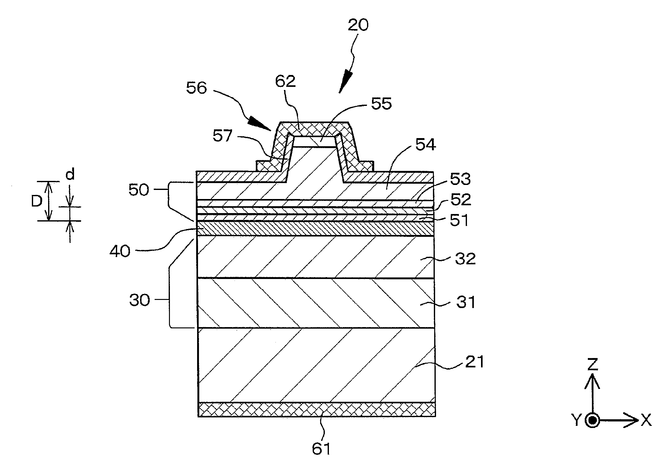
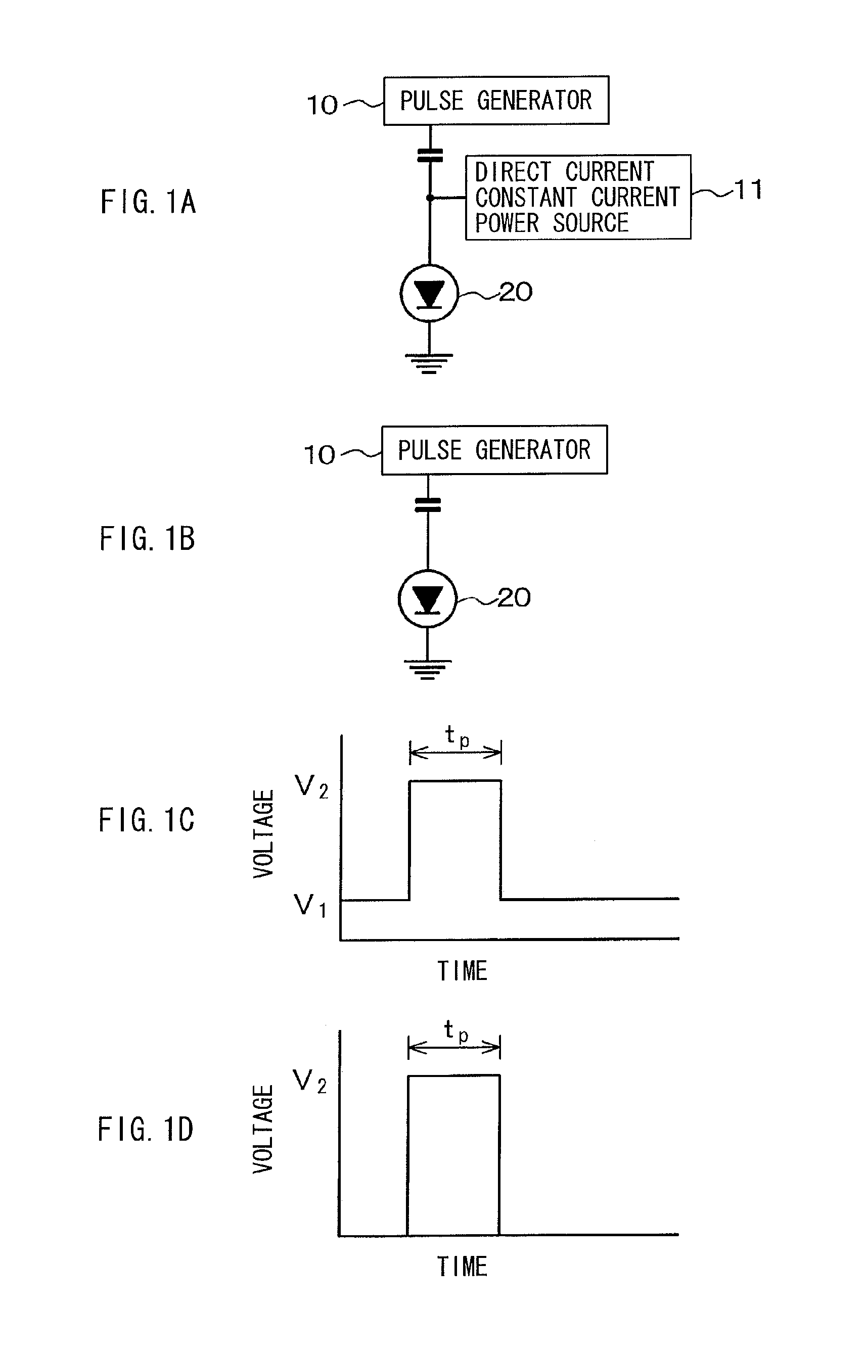
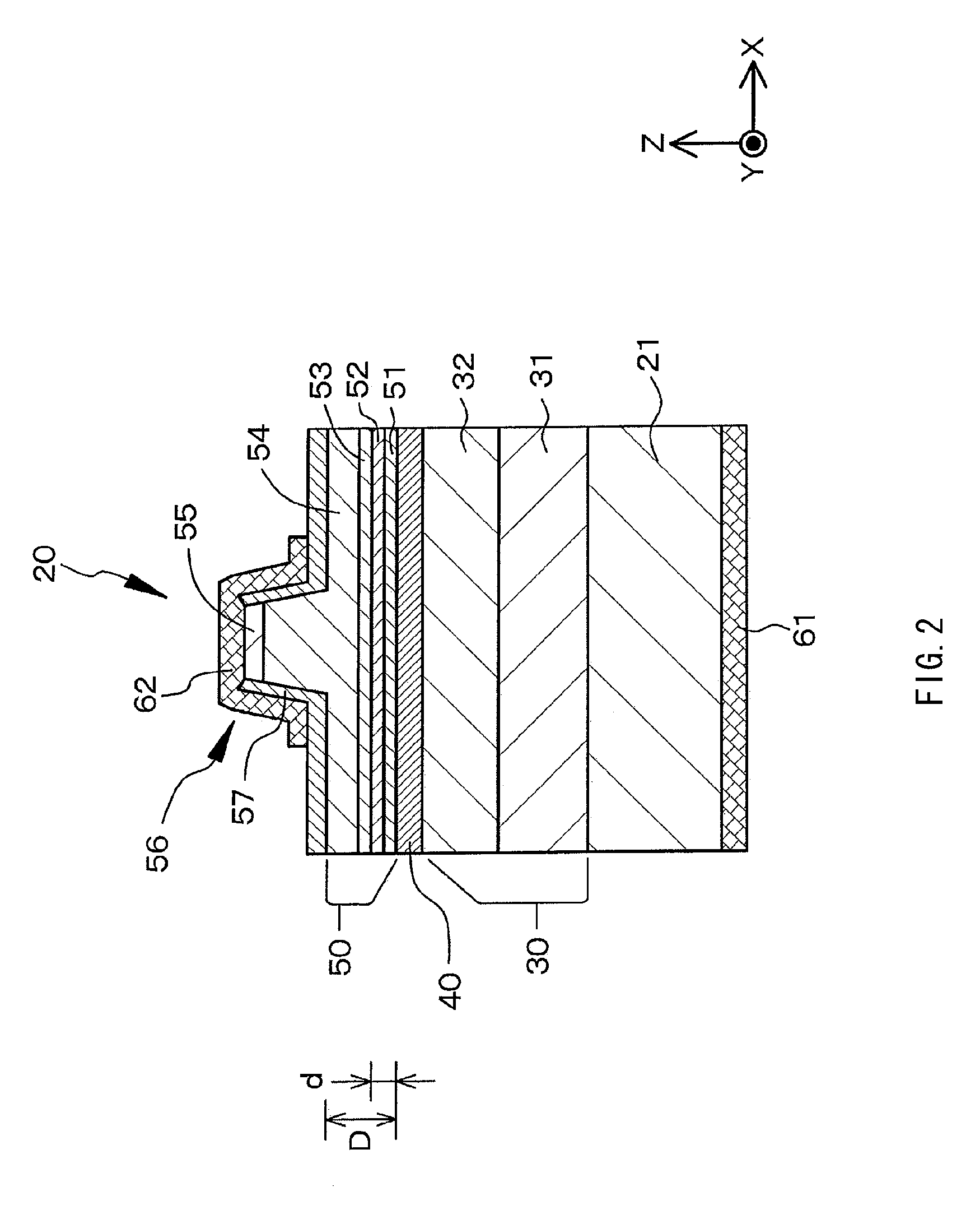
[0075]The first embodiment relates to the laser diode device, the method of driving the same, and the laser diode apparatus according to the first aspect of the invention and the second aspect of the invention, and further relates to the first structure laser diode device, the second structure laser diode device, and the fourth structure laser diode device. A conceptual diagram of the laser diode apparatus of the first embodiment is illustrated in FIG. 1A or FIG. 1B. A rectangular pulse voltage applied to the laser diode device is schematically illustrated in FIG. 1C or FIG. 1D. A schematic cross sectional view of the laser diode device where the laser diode device is cut along a virtual perpendicular plane (YZ plane) perpendicular to the resonator direction (X direction) of the laser diode device of the first embodiment is illustrated in FIG. 2. A schematic cross sectional view of the laser diode device where the laser diode device is cut along a virtual perpendicular plane (XZ pla...

second embodiment

[0096]The second embodiment is a modified embodiment of the first embodiment. In the second embodiment, N pieces (in the second embodiment, N=2) of the carrier injection region and (N-1) pieces of the carrier non-injection region are provided, and the carrier injection regions sandwich the carrier non-injection region as a schematic cross sectional view of a laser diode device cut along a virtual perpendicular plane (XZ plane) including the resonator direction in FIG. 5. Otherwise, N pieces of the light emitting region (gain region) 40A and (N-1) piece of the saturable absorption region 40B are provided, and the light emitting regions 40A sandwich the saturable absorption region 40B.

[0097]Otherwise, in the laser diode device of the second embodiment, the second electrode 62 is separated into two sections by a separation trench 63. The width of the separation trench 63 is specifically 20 μm.

[0098]A composition and a structure of the laser diode device of the second embodiment are abl...

third embodiment

[0103]The third embodiment is also a modified embodiment of the first embodiment, and further relates to the third structure laser diode device. In the third embodiment, as a schematic cross sectional view of a laser diode device cut along a virtual perpendicular plane (XZ plane) including the resonator direction in FIG. 11, the second electrode is separated into a first section 62A and a second section 62B by the separation trench 63. The width of the separation trench is 20 μm. In the example illustrated in FIG. 11, two first sections 62A of the second electrode sandwich one second section 62B of the second electrode.

[0104]In the third embodiment, N pieces (in the third embodiment, N=2) of the carrier injection region and (N-1) pieces of the carrier non-injection region are provided, and the carrier injection regions sandwich the carrier non-injection region. Otherwise, N pieces of the light emitting region (gain region) 40A and (N-1) piece of the saturable absorption region 40B a...


PUM


Abstract

An ultrashort pulse and ultrahigh power laser diode device capable of outputting pulse laser light having higher peak power with a simple composition and a simple structure is provided. The laser diode device includes: a laminated structure composed of a first compound semiconductor layer containing n-type impurity, an active layer having a quantum well structure, and a second compound semiconductor layer containing p-type impurity; a first electrode electrically connected to the first compound semiconductor layer; and a second electrode electrically connected to the second compound semiconductor layer, wherein the second compound semiconductor layer is provided with an electron barrier layer having a thickness of 1.5*10−8 m or more, and driving is made by a pulse current having a value 10 or more times as large as a threshold current value.

Description

BACKGROUND OF THE INVENTION[0001]1. Field of the Invention[0002]The present invention relates to a laser diode device, a method of driving the same, and a laser diode apparatus.[0003]2. Description of the Related Art[0004]In these years, in the advanced scientific region researches using laser light with the pulse time on the attosecond time scale or on the femtosecond time scale, ultrashort pulse and ultrahigh power laser is actively used. As the ultrashort pulse and ultrahigh power laser, for example, titanium / sapphire laser is known. Such a titanium / sapphire laser is an expensive and large solid laser light source, which is a main factor to inhibit spread of the technology. If the ultrashort pulse and ultrahigh power laser is realized with the use of a laser diode, substantial miniaturization, price reduction, and high stability are able to be realized, which is expected to become a breakthrough for generalizing advanced scientific technology in this field.[0005]Meanwhile, short ...

Claims


Application Information

Patent Timeline
Patent Type & Authority Patents(United States)
IPC IPC(8): H01S5/00B82Y20/00H01S5/06H01S5/062H01S5/0625H01S5/20H01S5/343
CPCH01S5/06216B82Y20/00H01S5/0602H01S5/06253H01S5/2009H01S5/34333
Inventor KURAMOTO, MASARUOKI, TOMOYUKISUGAHARA, TOMOYAYOKOYAMA, HIROYUKI
Owner SONY CORP
Why Eureka
Try Eureka