Light-emitting semiconductor chip

a semiconductor chip and light-emitting technology, applied in semiconductor/solid-state device manufacturing, semiconductor devices, electrical apparatus, etc., can solve the problems of often not efficiently injected charge carriers into quantum wells, and achieve the effect of improving the behaviour of semiconductor chips

Active Publication Date: 2015-04-21
OSRAM OLED
View PDF42 Cites 8 Cited by
  • Summary
  • Abstract
  • Description
  • Claims
  • Application Information

AI Technical Summary

Benefits of technology

[0005]In one aspect, a semiconductor chip is designed so that charge carriers may be injected efficiently into the active region.
[0011]It has been found that a doping peak which, in particular in comparison with the rest of the extent of the n-conductive multilayer structure, is thin and highly doped, leads to improved charge carrier injection into the active region of the semiconductor chip. As a result of high doping, the n-conductive multilayer structure exhibits comparatively high transverse conductivity in the region of the doping peak, i.e., high conductivity in the lateral direction, such that charge carriers may be injected particularly homogeneously into the active region in the lateral direction. The at least one doping peak also results in laterally more homogeneous current flow in the reverse direction, i.e., the blocking direction of the active region. In this way, the semiconductor chips exhibit reduced sensitivity to electrostatic discharge (ESD).
[0033]By means of this highly doped doping peak in the vicinity of the active region, injection of charge carriers into the active region may take place particularly efficiently and in particular particularly homogeneously in the lateral direction. The at least one doping peak also brings about improved utilisation of a large number of possible charge carrier paths due to the high transverse conductivity, which reduces the risk of ESD damage compared to a semiconductor chip with no doping peaks in the n-conductive region of the semiconductor body.
[0035]In a preferred further development a crystal structure of the n-conductive multilayer structure comprises V-shaped indentations. Such indentations, which may form during deposition of the semiconductor layers in particular along dislocation lines, are also known as “V pits.” Such V-shaped indentations may form in particular at a comparatively low deposition temperature of the semiconductor material, for instance below 950° C. These V-shaped indentations may lead to improved behaviour of the semiconductor chip in the non-conducting direction.

Problems solved by technology

One cause of this is that the charge carriers are often not injected efficiently into the quantum wells.

Method used


Image

  • Light-emitting semiconductor chip
  • Light-emitting semiconductor chip
  • Light-emitting semiconductor chip

Examples


Embodiment Construction

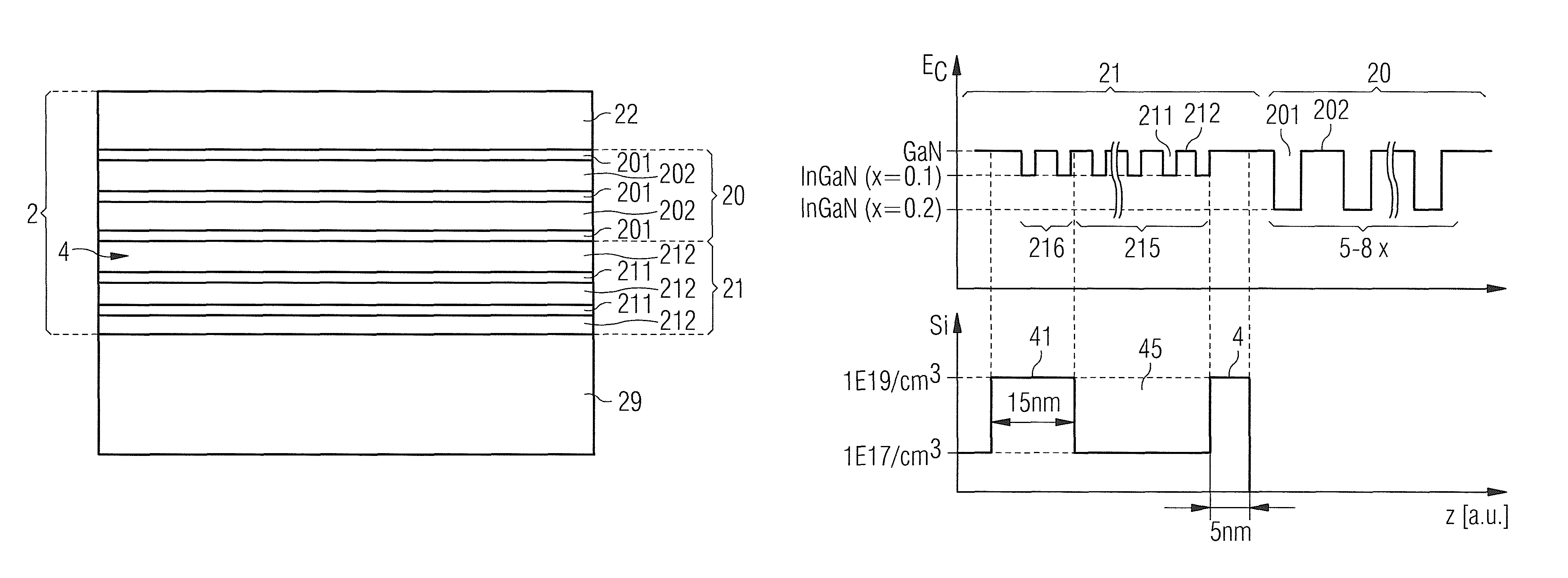
[0049]A first exemplary embodiment of a semiconductor body for a semiconductor chip is illustrated schematically in sectional view in FIG. 1A. The semiconductor body 2 comprises a semiconductor layer sequence which forms the semiconductor body. The semiconductor layer sequence comprises an active region 20 intended for generating radiation, which is arranged between an n-conductive multilayer structure 21 and a p-conductive semiconductor layer 22. The semiconductor layer sequence of the semiconductor body is preferably deposited epitaxially, in particular by MBE or MOCVD, on a growth substrate 29. Examples of materials suitable as a growth substrate for a semiconductor body based on a nitride compound semiconductor material are sapphire, silicon carbide, silicon or gallium nitride. A buffer layer may be formed between the n-conductive multilayer structure 21 and the growth substrate, which buffer layer may in particular be provided to enhance crystal quality (not shown explicitly).

[...


PUM


Abstract

A semiconductor chip includes a semiconductor body with a semiconductor layer sequence. An active region intended for generating radiation is arranged between an n-conductive multilayer structure and a p-conductive semiconductor layer. A doping profile is formed in the n-conductive multilayer structure which includes at least one doping peak.

Description

[0001]This patent application is a national phase filing under section 371 of PCT / EP2010 / 070761, filed Dec. 27, 2010, which claims the priority of German patent application 10 2009 060 747.1, filed Dec. 30, 2009, each of which is incorporated herein by reference in its entirety.TECHNICAL FIELD[0002]The present invention relates to a semiconductor chip intended for generating radiation.BACKGROUND[0003]LED semiconductor chips often have an active region intended for generating radiation, with a plurality of quantum wells.SUMMARY OF THE INVENTION[0004]It has become apparent that, when there are InGaN quantum wells in the active region, the radiant power emitted does not increase in a linear manner as the current density increases. One cause of this is that the charge carriers are often not injected efficiently into the quantum wells.[0005]In one aspect, a semiconductor chip is designed so that charge carriers may be injected efficiently into the active region.[0006]In one embodiment, a...

Claims


Application Information

Patent Timeline
Patent Type & Authority Patents(United States)
IPC IPC(8): H01L29/06H01L33/04H01L33/06H01L33/14H01L33/22H01L33/38
CPCH01L33/04H01L33/14H01L33/22H01L33/382H01L33/06H01L2224/16225H01L2924/0002H01L2924/00H01L33/24H01L33/0093H01L33/32
Inventor PETER, MATTHIASMEYER, TOBIASWALTER, ALEXANDERTAKI, TETSUYAOFF, JUERGENBUTENDEICH, RAINERHERTKORN, JOACHIM
Owner OSRAM OLED
Why Eureka
Try Eureka