Group III-V ferromagnetic/non-magnetic semiconductor heterojunctions and magnetodiodes

a ferromagnetic/non-magnetic semiconductor and heterojunction technology, applied in the field of group iiiv ferromagnetic/non-magnetic semiconductor heterojunctions and magnetodiodes, can solve the problems of limiting the scalability of such devices, limiting the practical limitations of size reduction, and restricting the potential use and development of such devices, so as to increase the magnitude of linear increase in magnetoresistance, increase the magnetic field, increase the magnitude of linear increas

Active Publication Date: 2015-05-05
NORTHWESTERN UNIV
View PDF9 Cites 1 Cited by
  • Summary
  • Abstract
  • Description
  • Claims
  • Application Information

AI Technical Summary

Benefits of technology

[0012]In part, this invention can also be directed to a method of monitoring magnetoresistance. Such a method can comprise providing a device of the sort more broadly described above; applying a voltage across the device; applying a magnetic field oriented with respect to a current through the device; and measuring magnetoresistance of such a current responsive to the applied magnetic field. Alternatively, as would be understood in the art, such a method can be used to measure voltage change upon applying a current. Regardless, in certain embodiments thereof, as can be achieved with various such device structures, magnetoresistance can increase with increasing magnetic field. Demonstrating such a relationship, magnetoresistance can be measured at a temperature from about 25 K to about 300 K. Regardless of temperature, various such embodiments can show magnetoresistance increasing substantially linearly with a magnetic field increasing from about 1.5 T to about 9 T. Such benefits associated with this invention can be especially advantageous at temperatures up to about or higher than 300 K. Likewise, various such embodiments of this invention demonstrate that the magnitude of a linear increase in magnetoresistance can increase with increasing applied current. Such benefits and results can be especially useful at high magnetic field strengths (e.g., up to about 9 T). Regardless, in conjunction with one or more of the device structures described herein, such a monitoring method can be enhanced by decreasing device dimension, to increase current density and increase magnetoresistance.

Problems solved by technology

However, such devices have, for the most part, utilized conventional semiconductors and are restricted in terms of potential use and development due to inherent limitation of such materials.
For instance, non-linear response to an applied magnetic field limits the scalability of such devices and places practical limitations on size reduction.
Such a limitation has typically required use of at least two such devices for multi-directional sensing.

Method used


Image

  • Group III-V ferromagnetic/non-magnetic semiconductor heterojunctions and magnetodiodes
  • Group III-V ferromagnetic/non-magnetic semiconductor heterojunctions and magnetodiodes
  • Group III-V ferromagnetic/non-magnetic semiconductor heterojunctions and magnetodiodes

Examples


example 1

[0041]P-type In1-xMn,As films were deposited at 480° C. by atmospheric pressure metal-organic vapor phase epitaxy on nominally undoped, n-type InAs (100) substrates to form the heterojunctions. Precursors used were trimethylindium (TMIn), 0.3% arsine (AsH3) in hydrogen and tricarbonyl(methylcyclopentadienyl)manganese (TCMn). A pre-growth anneal at 510° C. was carried out under an arsine overpressure in order to remove surface oxide from the InAs substrate. A detailed description of the growth conditions for (In,Mn)As films has previously been reported. See, A. J. Blattner, J. Lensch, and B. W. Wessels, Journal of Electronic Materials 30, 1408 (2001). Manganese concentrations were determined using standards-based energy dispersive x-ray spectroscopy (EDS). X-ray diffraction was used to verify phase purity of the (In,Mn)As films. Film thickness, as determined by profilometry, ranged from about 100—about 525 nm. Room temperature hole concentrations of (In,Mn)As films are on the order o...

example 2

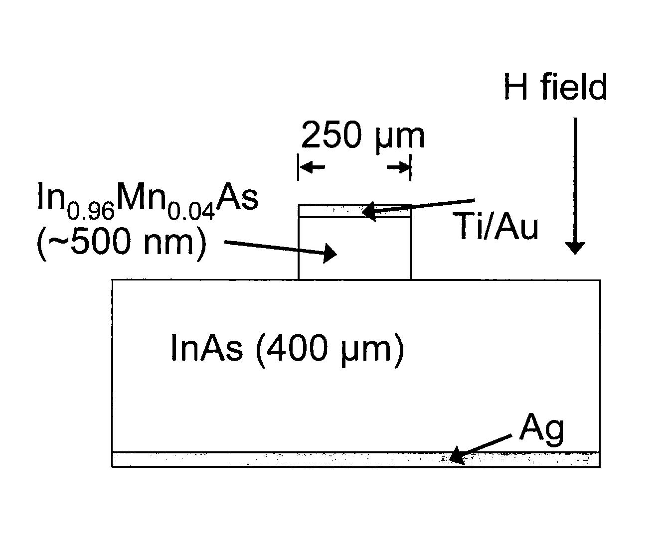
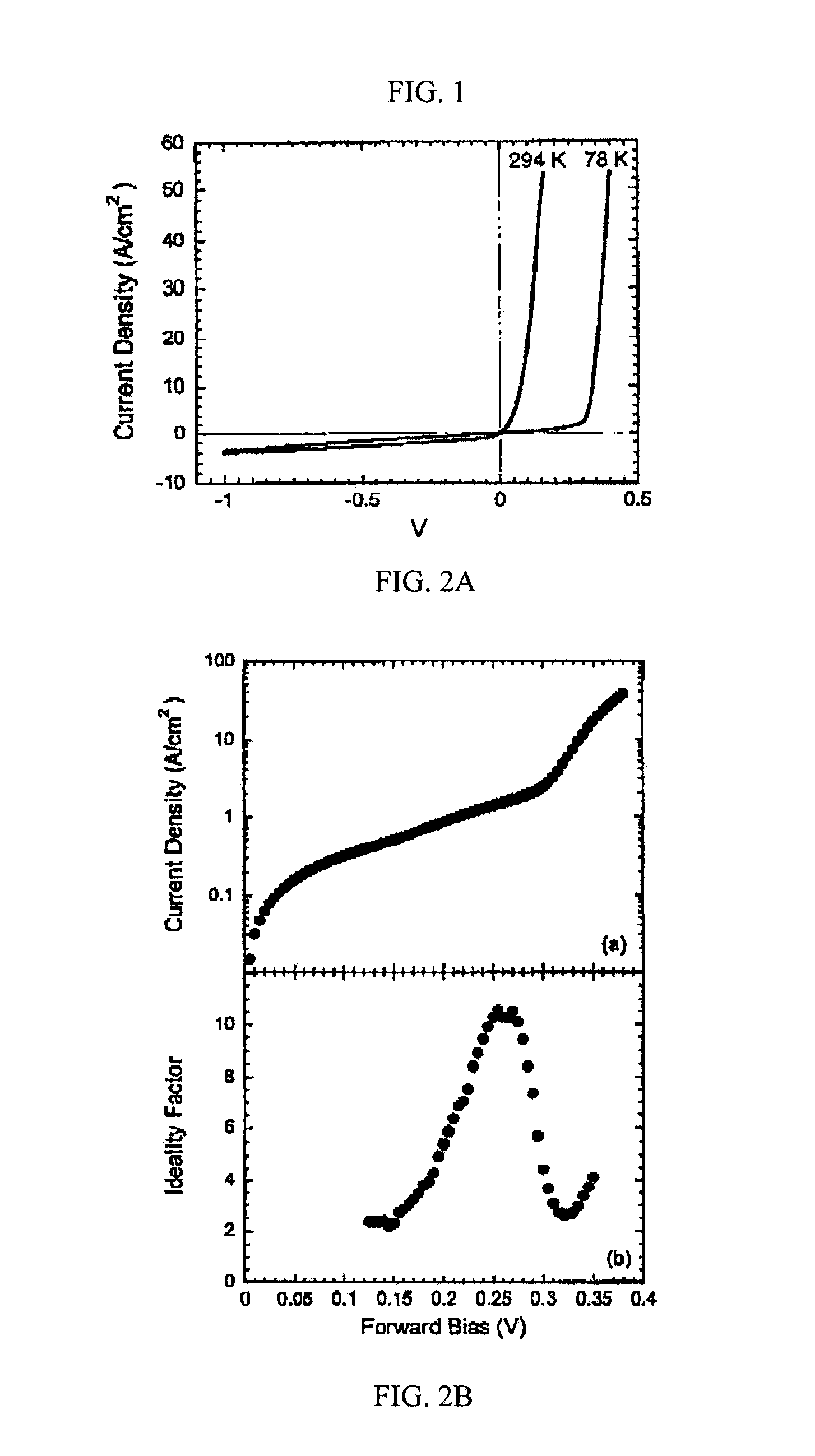
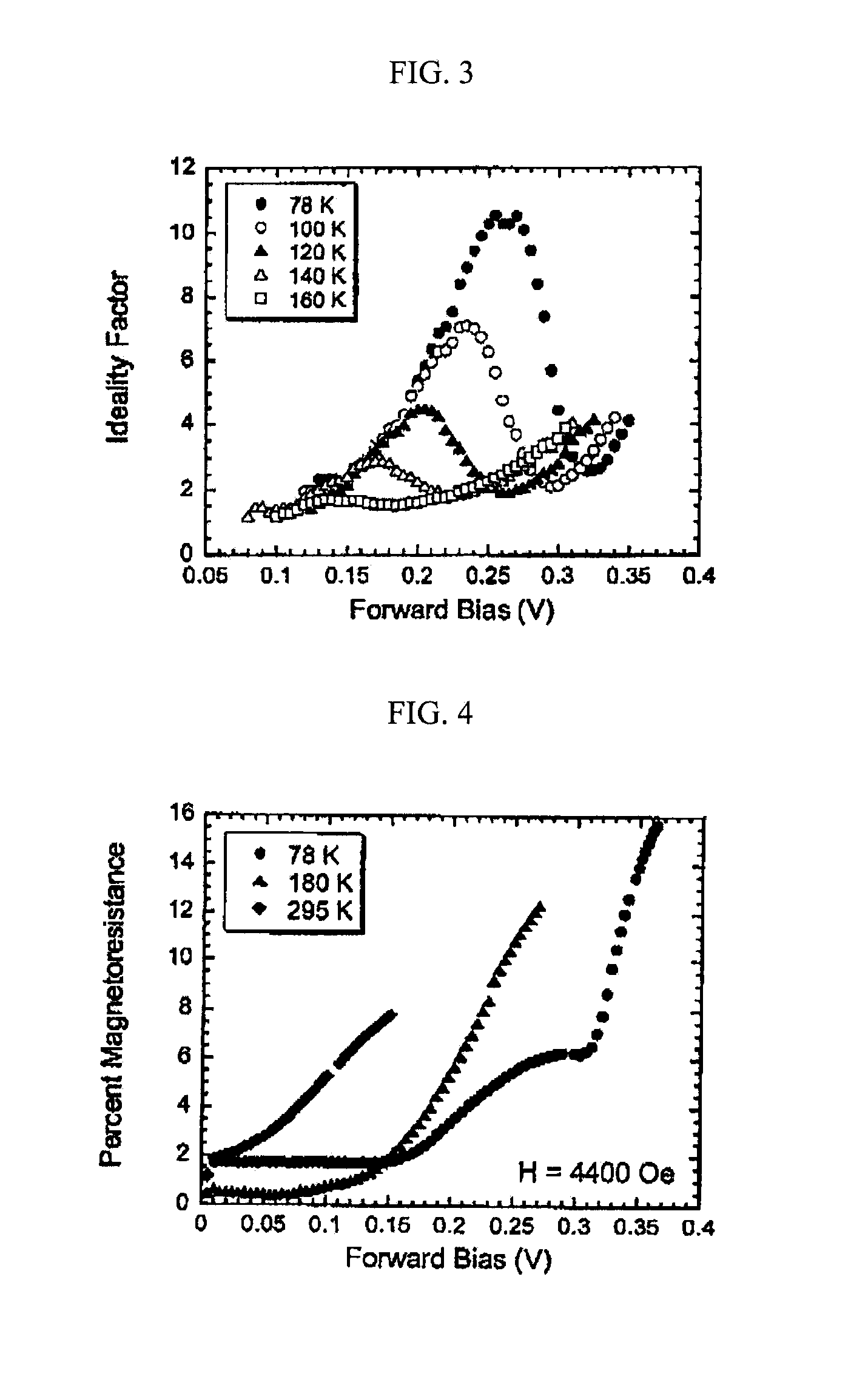
[0042]Mesa diodes were fabricated from the epitaxial structures using conventional photolithography and a citric acid wet etch. See, G. C. Desalvo, R. Kaspi, and C. A. Bozada, J. Electrochem. Soc. 141, 3526 (1994). The mesa diameter was 250 μm. Ti / Au (15 / 175 nm) ohmic contacts were evaporated to the (In,Mn)As films. Silver paste was used to make contact to the InAs substrates. The diodes were wire bonded to a non-magnetic chip carrier with gold wire. Low-temperature measurements were carried out in a Janis ST-100 cryostat with a non-magnetic sample holder. A Keithley 2400 source-meter was used to source voltages and measure currents. Magnetoresistance measurements were made in fields of up to 4600 Oe applied parallel to current flow across the junction.

[0043]Using a similar approach, high field, longitudinal magnetoresistance measurements were taken on a p-In0.96Mn0.04As / n-InAs junction. A nonsaturating linear magnetoresistance at fields greater than 1.5 T was observed at room tempe...

example 3

[0044]For these studies, a 500 nm thick p-In0.96Mn0.04As layer was deposited on an undoped n-InAs substrate using atmospheric pressure metal-organic vapor phase epitaxy under conditions previously described. (A. J. Blattner, J. Lensch, and B. W. Wessels, J. Electron. Mater. 30, 1408 (2001).) The room temperature electron concentration of the InAs substrate is 2×1016 cm−3, while the room temperature hole concentration of the p-InMnAs film is on the order of 1018-1019 cm−3. The diodes were patterned into 250 μm diameter mesas using photolithography and wet etching. Ti / Au was used as the p-In0.96Mn0.04As ohmic contact, while Ag was used as the n-InAs ohmic contact. Magnetoresistance measurements were made with the magnetic field applied parallel to the flow of current through the mesa diode using a Quantum Design Physical Properties Measurement System. A schematic of the experimental setup is shown in FIG. 7.


PUM


Abstract

Ferromagnetic Group III-V semiconductor / non-magnetic Group III-V semiconductor heterojunctions, with a magnetodiode device, to detect heterojunction magnetoresistance responsive to an applied magnetic field.

Description

[0001]This application is a divisional of and claims priority benefit from application Ser. No. 11 / 476,253 filed Jun. 27, 2006 now U.S. Pat. No. 7,956,608, which claimed priority benefit from application Ser. No. 60 / 694,420, filed Jun. 27, 2005, each of which is incorporated herein by reference in its entirety.[0002]This invention was made with government support under Grant No. DMR-0076097 awarded by the National Science Foundation and Grant No. ECS-0224210 awarded by the National Science Foundation. The government has certain rights in the invention.BACKGROUND OF THE INVENTION[0003]Magnetic sensors and magnetoresistive devices have been utilized in a wide variety of applications. However, such devices have, for the most part, utilized conventional semiconductors and are restricted in terms of potential use and development due to inherent limitation of such materials. For instance, non-linear response to an applied magnetic field limits the scalability of such devices and places pr...

Claims


Application Information

Patent Timeline
Patent Type & Authority Patents(United States)
IPC IPC(8): H01L21/02H01L29/267
CPCH01L29/267B82Y25/00G01R33/093G01R33/1284H10N50/10H10N50/85G01R33/1253
Inventor WESSELS, BRUCE W.MAY, STEVEN J.
Owner NORTHWESTERN UNIV
Why Eureka
Try Eureka