Method for manufacturing semiconductor device

a semiconductor and manufacturing method technology, applied in the field of semiconductor devices, can solve the problems of deterioration of electric characteristics of tft, long period of deposition time, etc., and achieve the effects of improving contrast, high quality, and favorable switching characteristics

Inactive Publication Date: 2015-06-09
SEMICON ENERGY LAB CO LTD
View PDF68 Cites 15 Cited by
  • Summary
  • Abstract
  • Description
  • Claims
  • Application Information

AI Technical Summary

Benefits of technology

[0015]In an inverted staggered TFT structure in which a semiconductor layer is provided over a gate electrode with a gate insulating film interposed therebetween, a semiconductor region which is formed in an early stage of deposition is used as a channel formation region. Accordingly, the higher the quality of the semiconductor region which is formed in the early stage of deposition is, the higher the electric characteristics, e.g., field-effect mobility of a TFT can be.
[0048]In addition, a liquid crystal display device using the thin film transistor which is obtained according to the manufacturing method of the present invention can increase field-effect mobility and thus can increase a driving frequency of a driver circuit. The driver circuit can be operated at high speed, so that a frame frequency can be quadruplicated or black frame insertion can be realized

Problems solved by technology

A low deposition rate results in a long period of deposition time.
Thus, there is a concern that more impurities are contained in the film during formation of the film, and those impurities cause deterioration in electric characteristics of a TFT.

Method used


Image

  • Method for manufacturing semiconductor device
  • Method for manufacturing semiconductor device
  • Method for manufacturing semiconductor device

Examples


embodiment mode 1

(Embodiment Mode 1)

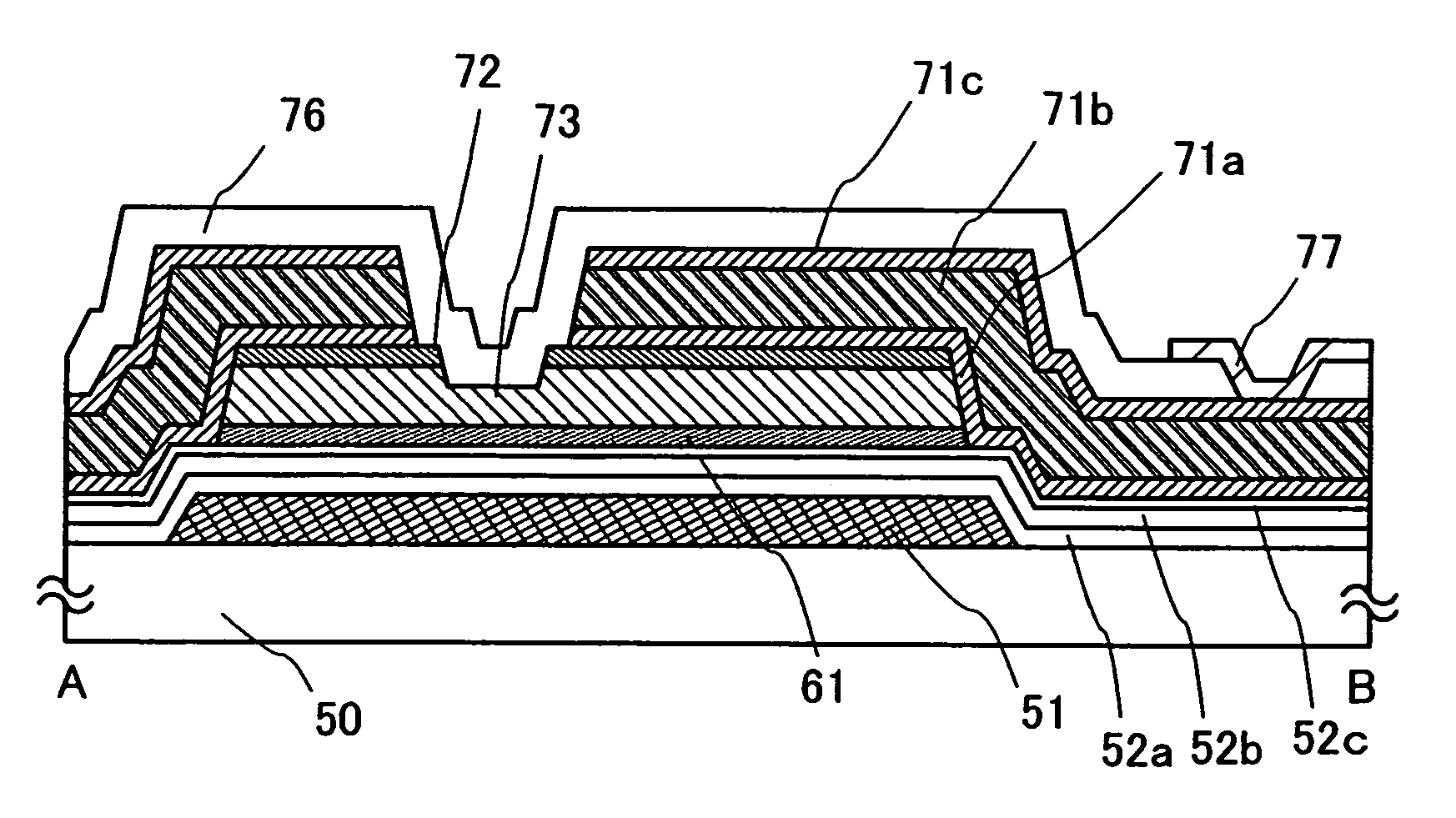
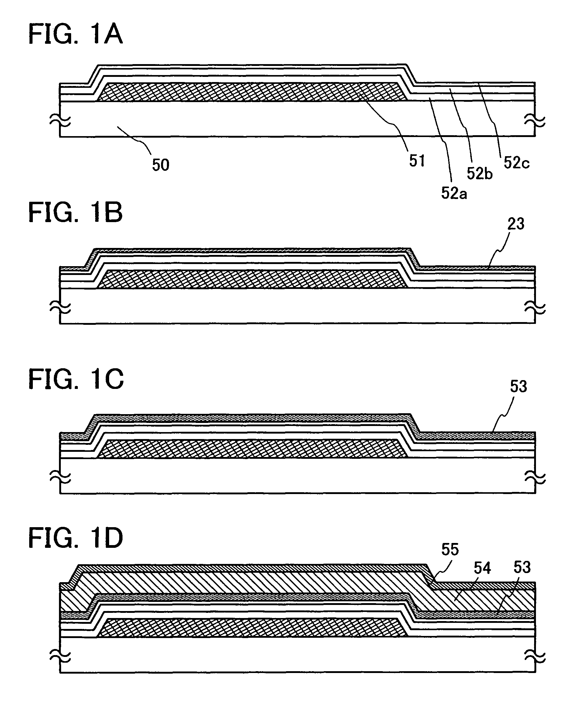
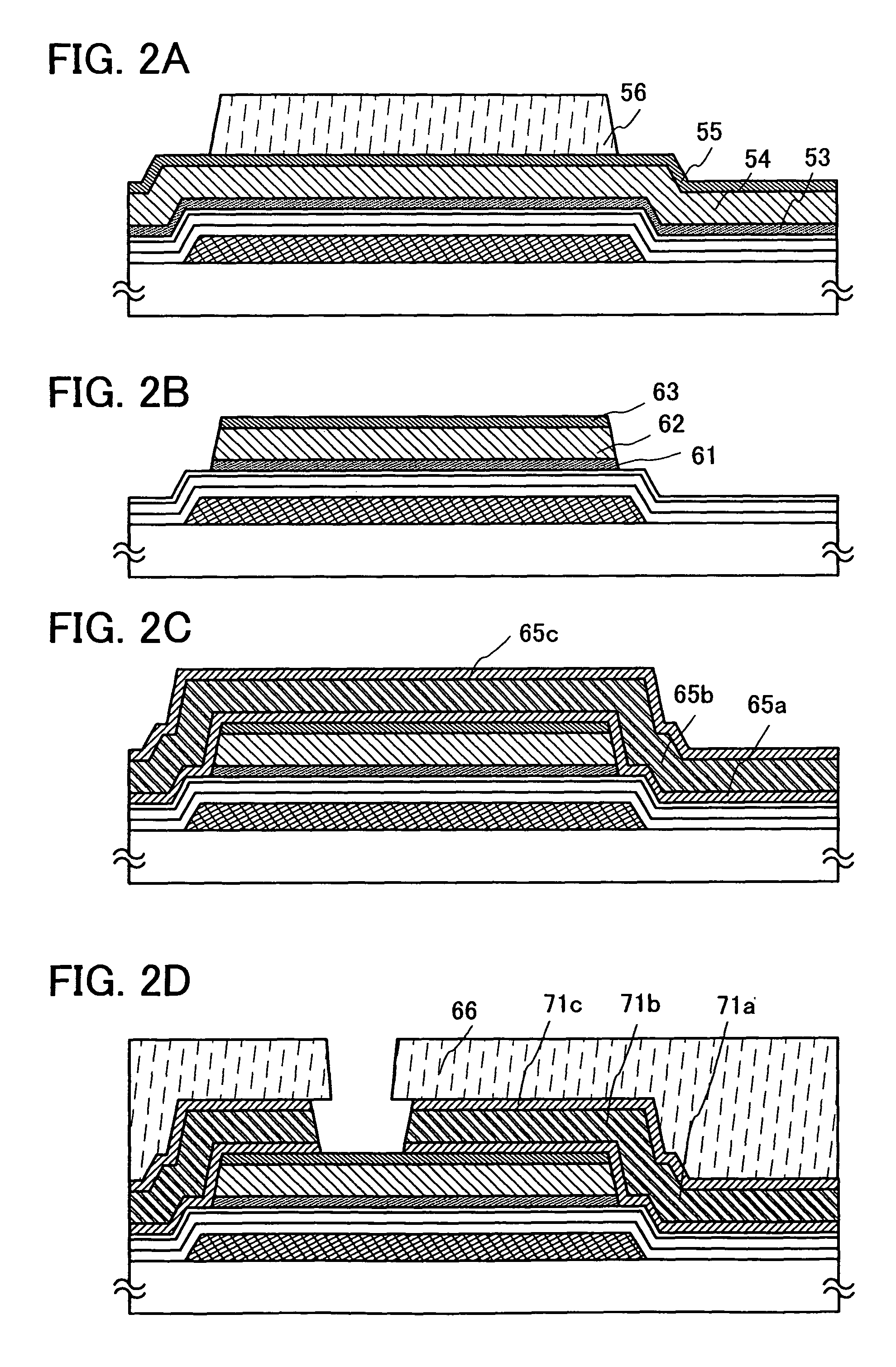
[0084]In this embodiment mode, a manufacturing process of a thin film transistor used for a liquid crystal display device will be described with reference to FIGS. 1A to 1D, FIGS. 2A to 2D, FIGS. 3A to 3C, FIG. 4, and FIG. 5. FIGS. 1A to 1D, FIGS. 2A to 2D, and FIGS. 3A to 3C are cross-sectional views showing a manufacturing process of a thin film transistor, and FIG. 4 is a top view showing a connection region of a thin film transistor and a pixel electrode in a single pixel. Further, FIG. 5 is a timing chart showing a formation method of a microcrystalline silicon film.

[0085]An n-channel thin film transistor having a microcrystalline semiconductor film is more suitable for use in a driver circuit than a p-channel thin film transistor having a microcrystalline semiconductor film, because the n-channel one has higher mobility. It is desired that all thin film transistors formed over the same substrate have the same polarity, in order to reduce the number of manufa...

embodiment mode 2

(Embodiment Mode 2)

[0146]This embodiment mode shows one example of a multi-chamber plasma CVD apparatus suitable for formation of a gate insulating film, a microcrystalline semiconductor film, and an n+ layer included in the TFT described in Embodiment Mode 1.

[0147]FIG. 6 shows one example of a multi-chamber plasma CVD apparatus provided with a plurality of reaction chambers. This apparatus is provided with a common chamber 123, a load / unload chamber 122, a first reaction chamber 100a, a second reaction chamber 100b, and a third reaction chamber 100c. This apparatus is a single wafer-processing type in which a substrate set in a cassette 124 in the load / unload chamber 122 is transferred to / from each reaction chamber by a transfer unit 126 in the common chamber 123. A gate valve 125 is provided between the common chamber 123 and each reaction chamber, so that processing in one reaction chamber does not affect processing in other reaction chambers.

[0148]The reaction chambers are sorte...

embodiment mode 3

(Embodiment Mode 3)

[0155]This embodiment mode will describe a manufacturing process of a thin film transistor using a multi-chamber plasma CVD apparatus which is different from that in FIG. 6 described in Embodiment Mode 2, with reference to FIG. 7. FIG. 6 shows the apparatus provided with three reaction chambers, whereas FIG. 7 is a top view of a multi-chamber plasma CVD apparatus provided with four reaction chambers.

[0156]FIG. 7 shows a structure in which a fourth reaction chamber 100d is provided in addition to the structure of the multi-chamber plasma CVD apparatus of FIG. 6. In FIG. 7, the same components as in FIG. 6 are denoted by the same reference numerals and detailed description thereof is omitted. Further, a combination of exhaust units shown in FIG. 7 is one example and the combination is not particularly limited thereto.

[0157]A gas supply unit 108b is connected to the fourth reaction chamber 100d. The structure of the high-frequency power supply units and the exhaust u...


PUM


Abstract

After a gate insulating film is formed over a gate electrode, in order to improve the quality of a microcrystalline semiconductor film which is formed in an early stage of deposition, a film near an interface with the gate insulating film is formed under a first deposition condition in which a deposition rate is low but the quality of a film to be formed is high, and then, a film is further deposited under a second deposition condition in which a deposition rate is high. Then, a buffer layer is formed to be in contact with the microcrystalline semiconductor film. Further, plasma treatment with a rare gas such as argon or hydrogen plasma treatment is performed before formation of the film under the first deposition condition for removing adsorbed water on a substrate.

Description

BACKGROUND OF THE INVENTION[0001]1. Field of the Invention[0002]The present invention relates to a semiconductor device including a circuit which is formed using a thin film transistor (hereinafter referred to as a TFT) and a manufacturing method thereof. For example, the present invention relates to an electronic device provided with, as a component, an electro-optical device typified by a liquid crystal display panel or a light-emitting display device having an organic light-emitting element.[0003]Note that in this specification, a semiconductor device refers to all types of devices which can function by utilizing semiconductor characteristics. An electro-optical device, a semiconductor circuit, and an electronic device are all included in the category of the semiconductor device.[0004]2. Description of the Related Art[0005]In recent years, a technique for forming thin film transistors (TFTs) using a semiconductor thin film (the thickness of several nm to several hundred nm) forme...

Claims


Application Information

Patent Timeline
Patent Type & Authority Patents(United States)
IPC IPC(8): H01L21/84H01L29/417H01L29/04H01L29/786H01L29/49H01L29/66H01L21/67H01L21/02H01L27/12
CPCH01L29/78696H01L29/04H01L29/41733H01L29/4908H01L29/66765H01L29/78678H01L21/02532H01L21/0262H01L21/67207H01L27/1288
Inventor YAMAZAKI, SHUNPEITEDUKA, SACHIAKITORIUMI, SATOSHIFORUNO, MAKOTOJINBO, YASUHIRODAIRIKI, KOJIKUWABARA, HIDEAKI
Owner SEMICON ENERGY LAB CO LTD
Why Eureka
Try Eureka