

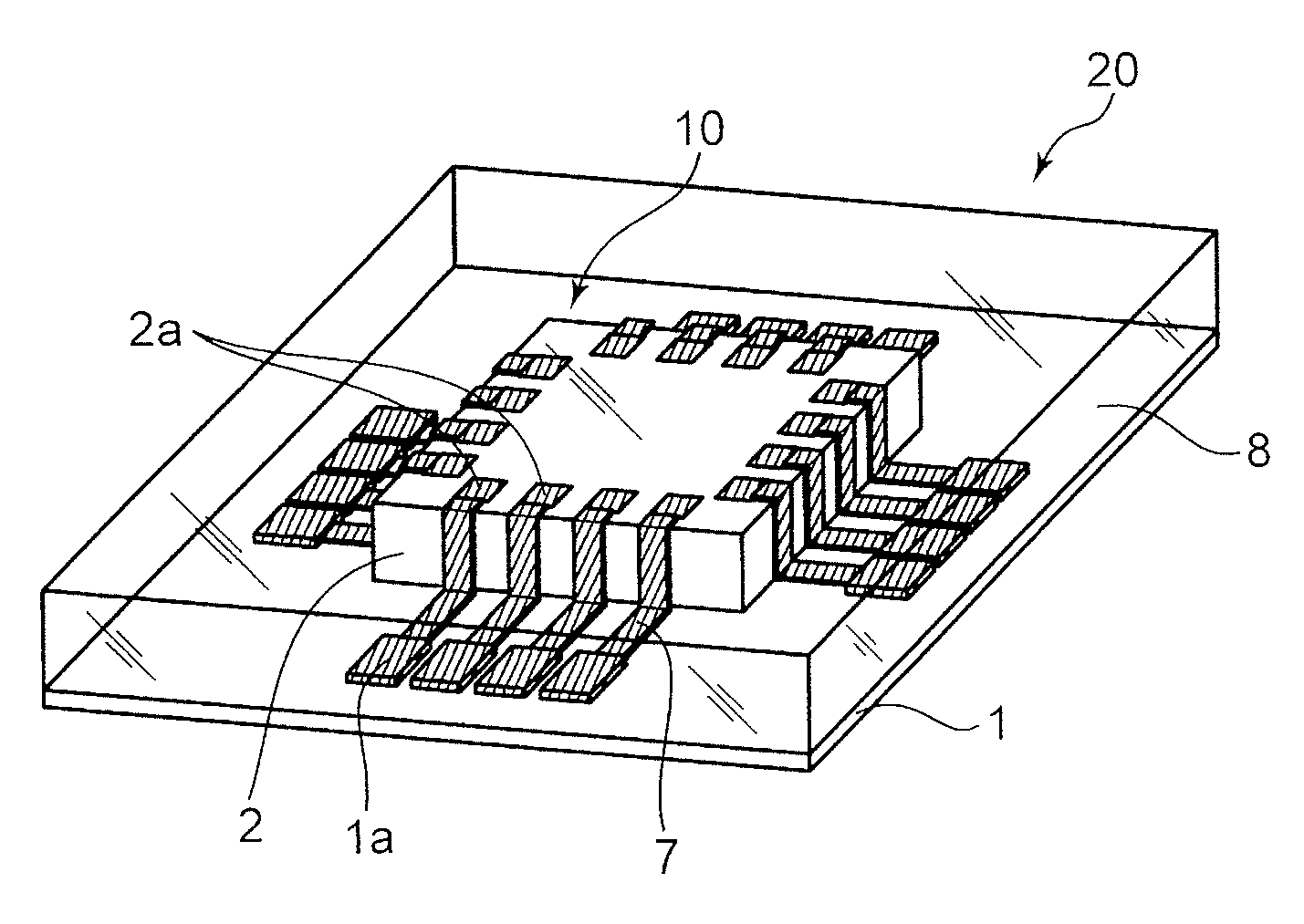
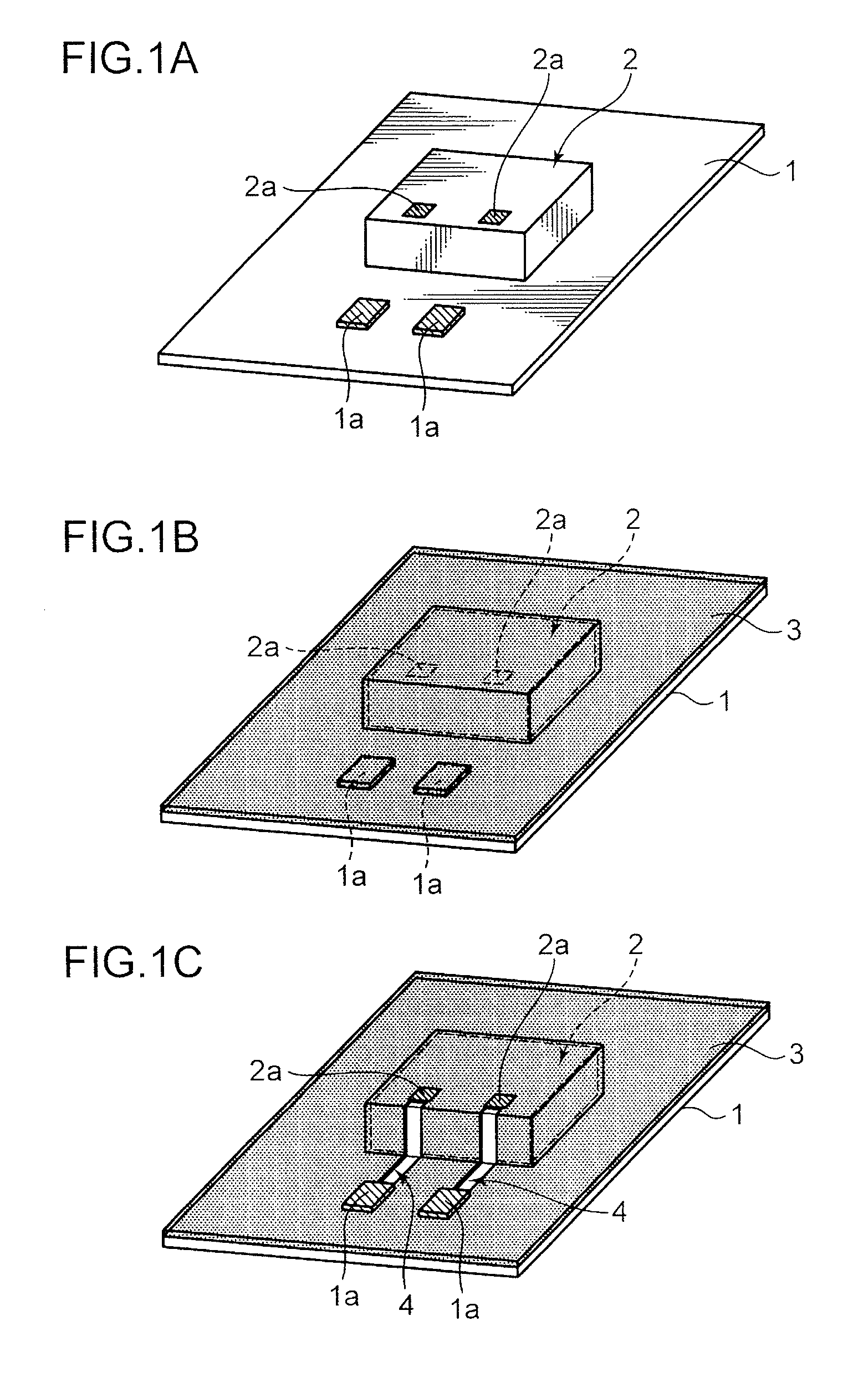
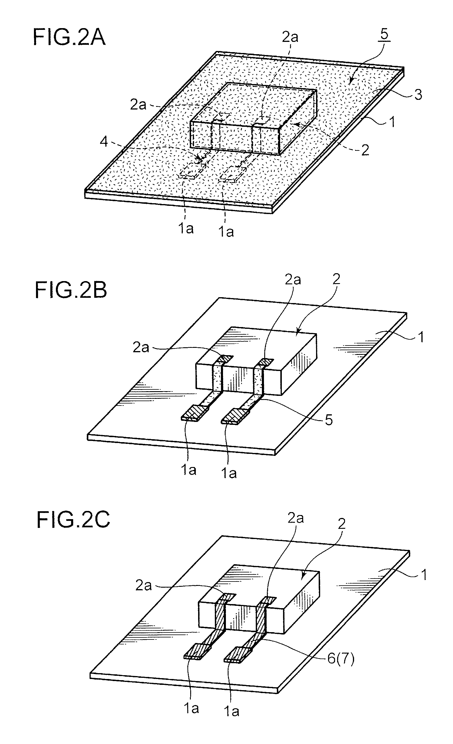
Three-dimensional structure in which wiring is provided on its surface
a three-dimensional structure and surface technology, applied in the direction of sustainable manufacturing/processing, semiconductor/solid-state device testing/measurement, instruments, etc., can solve the problems of high cost of gold wires, inability to meet the requirements of use, so as to inhibit the breakage or damage of wires
- Summary
- Abstract
- Description
- Claims
- Application Information
AI Technical Summary
Benefits of technology
Problems solved by technology
Method used
Image

Examples
example 1
[0267]First of all, the insulating resin layer was formed on a supporting substrate.
[0268]As a material for the insulating resin layer, a resin composition that contains bisphenol A-type epoxy resin (“850S” manufactured by DIC Corporation), multifunctional epoxy resin (“VG310108M” manufactured by Printec Corporation), dicyandiamide as a curing agent (“DICY” manufactured by Nippon Carbide Industries Co., Inc.), 2-ethyl-4-methylimidazole as a curing accelerator (“2E4MZ” manufactured by Shikoku Chemicals Corporation), spherical fused silica as an inorganic filler (“FB1SDX” with an average particle size of 1.7 μm, manufactured by Denki Kagaku Kogyo Kabushiki Kaisha), a silane coupling agent (“A-187” manufactured by Momentive Performance Materials Inc.), methyl ethyl ketone (MEK) as a solvent, and N,N-dimethylformamide (DMF), was used.
[0269]Three of this sheet-like insulating resin layer (with a thickness of 100 μm) configured by this resin composition were stacked and placed on a circui...
example 2
[0286]Example 2 was executed in the same manner as Example 1, except that a carboxyl group-containing polymer (manufactured by Zeon Corporation, with an acid equivalent of 500, a weight-average molecular weight of 25000, and a solid content of 20%) was used in place of the methyl ethyl ketone (MEK) suspension of styrene-butadiene copolymer (SBR) (manufactured by Zeon Corporation, with an acid equivalent of 600, a particle size of 200 nm, and a solid content of 15%).
[0287]At that moment, the swelling level relative to the sodium hydroxide aqueous solution having a concentration of 5% and pH 14 was 1000%. On the other hand, the swelling level relative to the hydrochloric acid aqueous solution having a concentration of 5% and pH 1 was 30%.
[0288]As a result, a three-dimensional structure (wiring substrate) that is as excellent as that of Example 1 was obtained.
PUM
| Property | Measurement | Unit |
|---|---|---|
| width | aaaaa | aaaaa |
| width | aaaaa | aaaaa |
| diameter | aaaaa | aaaaa |
Abstract
Description
Claims
Application Information