Balanced barrier discharge neutralization in variable pressure environments

Active Publication Date: 2015-07-14
ILLINOIS TOOL WORKS INC
View PDF10 Cites 19 Cited by
  • Summary
  • Abstract
  • Description
  • Claims
  • Application Information

AI Technical Summary

Benefits of technology

[0006]The unavoidable generation of electrostatic charges in middle and low pressure roll to roll semiconductor manufacturing environments presents significant problems. These include (1) electrostatic adhesion of the thin film due to handling and/or guiding devices during loading and/or unloading, (2) damaged thin film work product due to high electrical stresses and discharges, and (3) thin film surface contamination due to adhesion of attracted particulates. These problems are expected to become more acute as semiconductor circuitry dimensions decrease and densities increase. Thus, there is growing interest in electrostatic charge generation, monitoring, and neutralization, especially in low pressure roll to roll semiconductor manufacturing.
[0007]Corona-based static charge neutralizers designed to operate at normal atmospheric pressure (typically about 760 Torr) are, of course, well known. However, they are generally considered to be undesirable for use in variable and/or middle to low pressure environments because they are prone to electrical breakdowns, spark discharges, and electrode erosion. For these reasons, other technologies have been adopted for use in low pressure semiconductor manufacturing. For example, plasma neutralizers using magnetron-DC discharge or RF type plasma ion generating sources have been used to shower semiconductor wafers with electron/ion beams during ion implantation and/or etching. Also, photo ionizing neutralizers using soft X-ray and UV light generating lamps are known for neutralizing products at low pressure in the presence of inert and electro-positive gases like N2 and Ar. However, the efficiency of photo ionizing neutralizers is known to dramatically decrease at N2 and O2 gas pressures in the range 10−1-10−2 Torr. Finally, UV deuterium lamp neutralizers may provide bipolar ionization and static charge reduction on wafers at reduced pressure down to 10−3-10−5 Torr. Such neutralizers suffer from a number of serious deficiencies. These include the fact that UV deuterium arc lamps (1) operate at very high temperatures, (2) require special high voltage power supplies and efficient cooling systems, and (3) produce relatively narrow neutralization beams that operate across small areas.
[0008]Accordingly, further improvements in static charge neutralization in thin film and/or wafer semiconductor manufacturing, especially as performed in middle to low vacuum pressure environments, continue to be desirable.
[0009]One aspect of the present invention is directed to a balanced ionizer for static charge neutralization in a variable pressure environment in response to the application of variable-waveform signals thereto. The balanced ionizer may comprise (1) a hollow dielectric channel having a length and an outer surface, the dielectric channel being disposed within the variable pressure environment; (2) a reference emitter helically disposed along the length of and on the outer surface of the dielectric channel, the reference emitter receiving a variable-waveform reference signal dictated by conditions in the variable pressure environment; and (3) a high voltage electrode disposed within the hollow dielectric channel. In accordance with the invention, the high voltage electrode may present a high intensity electric field to the reference emitter through the dielectric channel in response to the provision of a variable-waveform high voltage signal dictated by conditions in the variable pressure environment. That electric field may cause the generation of a plasma region w

Problems solved by technology

The unavoidable generation of electrostatic charges in middle and low pressure roll to roll semiconductor manufacturing environments presents significant problems.
These include (1) electrostatic adhesion of the thin film due to handling and/or guiding devices during loading and/or unloading, (2) damaged thin film work product due to high electrical stresses and discharges, and (3) thin film surface contamination due to a

Method used


Image

  • Balanced barrier discharge neutralization in variable pressure environments
  • Balanced barrier discharge neutralization in variable pressure environments
  • Balanced barrier discharge neutralization in variable pressure environments

Examples


Embodiment Construction

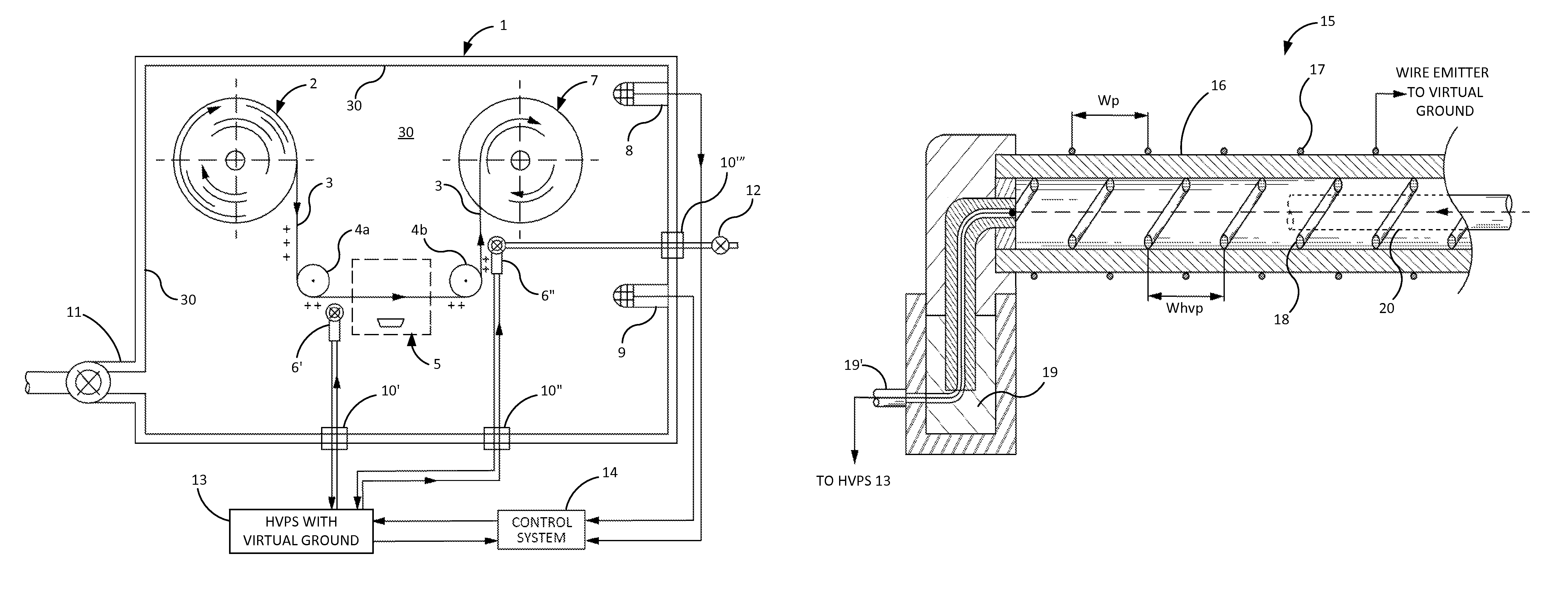
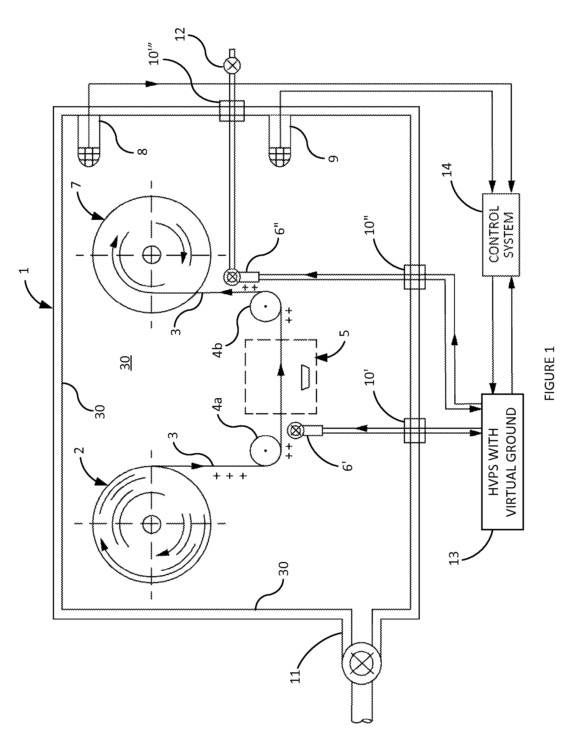
[0028]With reference to FIG. 1, a simplified representation of a middle or low pressure (i.e., deep vacuum) chamber 1 is bounded on all sides by chamber walls 30 and equipped with a barrier discharge neutralizer system in accordance with the present invention. Generally, the neutralizer system comprises ionization cells 6′ and 6″ electrically linked to a high voltage power supply 13 (which, in turn, is communicatively linked to a control system 14). As is typical, chamber 1 is equipped with process monitoring devices such as a pressure gauge / sensor 8 or / and a residual gas analyzer 9 that are communicatively linked to conventional control system 14 (which, in turn, is communicatively linked to high voltage power supply 13). In this way, environmental condition sensors, such as pressure sensor 8 and / or ozone sensor 40, may sense at least one environmental condition within the environment (e.g., a variable pressure environment), and HVPS 13 may produce variable-waveform high-voltage si...


PUM


Abstract

Methods and apparatus for static charge neutralization in variable pressure environments are disclosed. In particular, barrier discharge ionization apparatus may include a hollow dielectric channel disposed within a variable pressure environment and may have at least one open end, a reference emitter disposed on the outer surface of the channel, and a high voltage electrode disposed within the channel. The high voltage electrode may present a high intensity electric field to the reference emitter through the dielectric channel in response to the provision of a variable-waveform signal dictated by conditions in the variable pressure environment. This results in the generation of a plasma region with electrically balanced charge carriers within the variable pressure environment due to barrier discharge occurring at the interface of the reference emitter and the outer surface of the dielectric channel. The disclosed apparatus are compatible with either radio frequency or micro-pulse voltage power supplies.

Description

BACKGROUND OF THE INVENTION[0001]1. Field of the Invention[0002]The present invention is directed to balanced ionization for static charge neutralization by barrier discharge. Accordingly, the general objects of the invention are to provide novel systems, methods, and apparatus of such character.[0003]2. Description of the Related Art[0004]A significant portion of present semiconductor manufacturing begins with the creation of wafers that are then processed in various ways in a low-pressure / vacuum environment. Such processing may include thin film material deposition, etching, spattering, plasma treatment, and / or other operations running at middle or deep vacuum (i.e., low pressure). In this context middle or deep vacuum pressure is typically between about 10−2 Torr to about 10−3 Torr.[0005]One new trend in semiconductor manufacturing is a transition away from wafer-based manufacturing and to continuous roll to roll manufacturing. Roll to roll semiconductor manufacturing generally e...

Claims


Application Information

Patent Timeline
IPC IPC(8): H05F3/00H05F3/06H05F3/04
CPCH05F3/06H01J37/32082H01J37/32348H01J37/3277H01J37/32935H01T23/00H05H1/2465H05F1/00
Inventor GEFTER, PETEROLDYNSKI, EDWARD ANTHONYHEYMANN, STEVEN BERNARD
Owner ILLINOIS TOOL WORKS INC
Why Eureka
Try Eureka