Semiconductor device and manufacturing method thereof

a semiconductor device and manufacturing method technology, applied in the direction of semiconductor devices, electrical devices, transistors, etc., can solve the problems of obvious deformation of electrical characteristics of semiconductor devices, especially increase in leakage current, and method is not sufficient to reduce leakage current, so as to achieve low etching selection ratio, reduce or reduce the effect of electric characteristic variation

Active Publication Date: 2015-08-11
SEMICON ENERGY LAB CO LTD
View PDF136 Cites 3 Cited by
  • Summary
  • Abstract
  • Description
  • Claims
  • Application Information

AI Technical Summary

Benefits of technology

[0007]However, in some cases, the electric characteristics of the transistor that includes a semiconductor having wide band gap and low carrier density as an active layer are decreased due to moisture or atmospheric components entering the semiconductor layer from the outside. Specifically, in some cases, the threshold value of the transistor is shifted, whereby the leakage current thereof is increased.
[0011]When the above-described structure is employed for a transistor including a wide band gap semiconductor layer, the wide band gap semiconductor layer can be separated into an island shape by a second insulating layer. Therefore, for example, leakage current flowing between adjacent transistors can be reduced.
[0015]The edge portion of the wide band gap semiconductor layer is in contact with the second insulating layer with passivation properties. Thus, external moisture or atmospheric components can be prevented from entering from the edge portion of the wide band gap semiconductor layer. As a result, a semiconductor device in which a decrease or a variation in electric characteristics is not easily caused can be obtained.
[0020]Silicon and silicon nitride have a high etching selection ratio with respect to an oxide semiconductor. Thus, when a material of one of silicon and silicon nitride is used for a stopper film and a step for removing the stopper film by etching is performed, a surface of an oxide semiconductor that is an active layer is not seriously damaged. Accordingly, a semiconductor device in which a decrease or a variation in electric characteristics is not easily caused can be manufactured.

Problems solved by technology

However, as a demerit of miniaturization of a semiconductor device, degradation of electrical characteristics of a semiconductor device, especially an increase in leakage current, is obvious (Patent Document 1).
However, the method is not sufficient for reducing a leakage current.

Method used


Image

  • Semiconductor device and manufacturing method thereof
  • Semiconductor device and manufacturing method thereof
  • Semiconductor device and manufacturing method thereof

Examples


embodiment 1

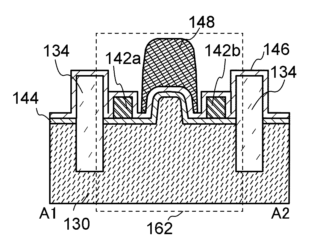
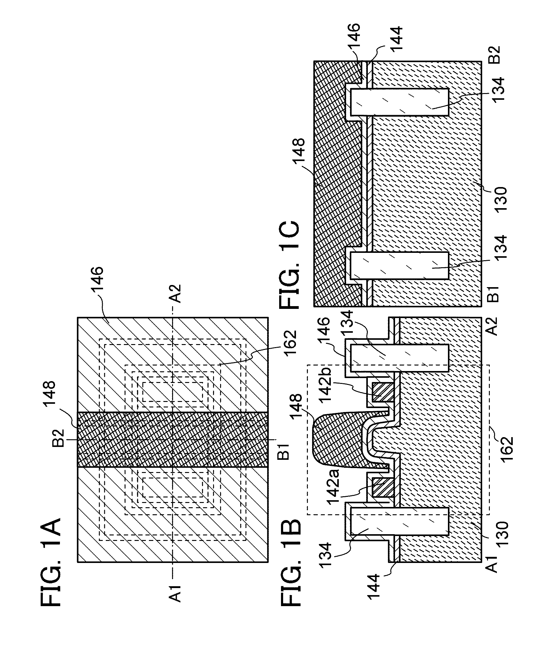
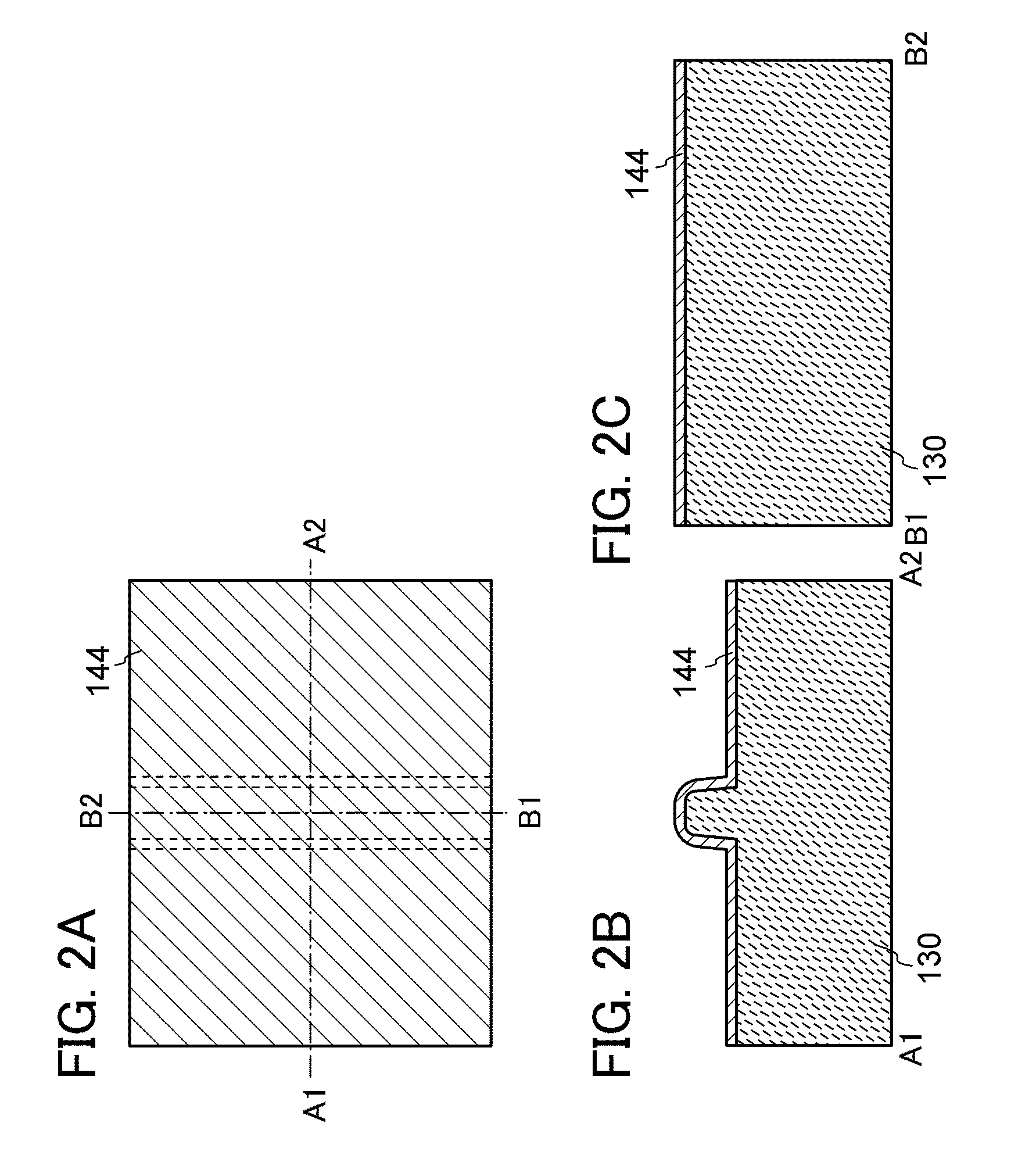
[0036]In this embodiment, a structure of a semiconductor device of one embodiment of the present invention is described with reference to FIGS. 1A to 1C. FIG. 1A illustrates an example of a top view of a transistor 162 of this embodiment, and FIGS. 1B and 1C illustrate a cross sectional view taken along dotted-dashed line A1-A2 and a cross sectional view taken along dotted-dashed line B1-B2 in FIG. 1A, respectively.

[0037]The transistor 162 described in this embodiment includes a first insulating layer 130, a wide band gap semiconductor layer 144 provided in contact with the first insulating layer 130, a source electrode (or drain electrode) 142a provided in contact with the wide band gap semiconductor layer 144, a drain electrode (or source electrode) 142b provided in contact with the wide band gap semiconductor layer 144, a second insulating layer 134 that separates the wide band gap semiconductor layer 144 into an island shape, a gate insulating layer 146 provided over the wide ba...

embodiment 2

[0072]In this embodiment, a structure and a manufacturing method in the case where the wide band gap semiconductor layer 144 described in Embodiment 1 as an example includes an oxide semiconductor are described.

[0073]In this embodiment, the structures of the wide band gap semiconductor layer 144, the first insulating layer 130, the gate insulating layer 146, the gate electrode 148, and the stopper film 150 are different from those in Embodiment 1. Hereinafter, the structures are explained. Description in Embodiment 1 can be referred to for the other structures.

[0074]In this embodiment, an example in which an oxide semiconductor is used for the wide band gap semiconductor layer 144 described in Embodiment 1 is described. Hereinafter, the layer is referred to as an oxide semiconductor layer.

(Oxide Semiconductor)

[0075]The oxide semiconductor layer is a thin film deposited to have a thickness of greater than or equal to 1 nm and less than or equal to 100 nm.

[0076]A material that can be ...

embodiment 3

[0124]In this embodiment, a structure and a manufacturing method in the case where a c-axis aligned crystalline (CAAC) oxide semiconductor layer is used for the wide band gap semiconductor layer 144 of the semiconductor device described in Embodiment 1 are described. Note that a CAAC oxide semiconductor layer is described in detail in Structure Example of Semiconductor Device.

[0125]A semiconductor device described in this embodiment is different from the semiconductor device described in Embodiment 1 in structures of the first insulating layer 130, a CAAC oxide semiconductor layer, the gate insulating layer 146, the gate electrode 148, and the stopper film 150. Thus, in this embodiment, structures and manufacturing methods of the first insulating layer 130, the CAAC oxide semiconductor layer, the gate insulating layer 146, the gate electrode 148, and the stopper film 150 are described. Description in Embodiment 1 can be referred to for the structures and the manufacturing methods of...


PUM


Abstract

In a transistor including a wide band gap semiconductor layer as a semiconductor layer, a wide band gap semiconductor layer is separated into an island shape by an insulating layer with passivation properties for preventing atmospheric components from permeating. The edge portion of the island shape wide band gap semiconductor layer is in contact with the insulating film; thus, moisture or atmospheric components can be prevented from entering from the edge portion of the semiconductor layer to the wide band gap semiconductor layer.

Description

BACKGROUND OF THE INVENTION[0001]1. Field of the Invention[0002]The present invention relates to a semiconductor device and a manufacturing method thereof.[0003]2. Description of the Related Art[0004]It is considered that a semiconductor device with low power consumption is more and more important for long battery life or for eco-friendly goods. In order to manufacture such a semiconductor device with low power consumption, a semiconductor device has been miniaturized. However, as a demerit of miniaturization of a semiconductor device, degradation of electrical characteristics of a semiconductor device, especially an increase in leakage current, is obvious (Patent Document 1).[0005]In order to reduce a leakage current, in a semiconductor device including silicon as a semiconductor layer, specifically, a field-effect transistor, a junction depth of a source region and a drain region that are adjacent to a channel region of the transistor is made to be shallow. However, the method is ...

Claims


Application Information

Patent Timeline
Patent Type & Authority Patents(United States)
IPC IPC(8): H01L29/12H01L21/8256H01L27/06H01L27/12H01L29/786H01L21/8252H01L21/336
CPCH01L21/8252H01L21/8256H01L27/0605H01L29/78603H01L29/7869H01L29/78696H01L27/1225
Inventor SASAGAWA, SHINYAISHIZUKA, AKIHIROHATANO, TAKEHISA
Owner SEMICON ENERGY LAB CO LTD
Why Eureka
Try Eureka