Phase-coupled arrays of nanowire laser devices and method of controlling an array of such devices

a technology of phase-coupled arrays and laser devices, which is applied in the direction of semiconductor lasers, instruments, optical elements, etc., can solve the problems of overall system drift and instability, and the research into phase-coupled arrays of (non-nanowire) semiconductor lasers is largely theoretical

Active Publication Date: 2015-08-11
STC UNM
View PDF14 Cites 34 Cited by
  • Summary
  • Abstract
  • Description
  • Claims
  • Application Information

AI Technical Summary

Benefits of technology

[0009]Another embodiment of the present disclosure is directed to a method of forming an array of nanowire devices. Each nanowire device is configured to exhibit lasing action when operated at increased current density. The array of nanowire devices comprises forming an LED array comprising a plurality of LED core-shell structures. Each LED core-shell structure comprises: a doped buffer layer disposed on a substrate, a first dielectric, disposed on the doped buffer layer, a nanowire core formed on the doped buffer layer through the first dielectric, and a layered shell formed to envelop the nanowire core, wherein the layered shell comprises a multi-quantum-well (MQW) active region. The method of forming the array of nanowire devices further comprises forming a p-side semiconductor to envelop the layered shell of each LED core-shell structure. A p-side electrode is formed having a thickness ranging from about 100 nm to about 500 nm to envelop the p-side semiconductor. A second dielectric material is formed between adjacent p-side electrodes for an electrical isolation, providing a surface comprising both the p-side electrodes and the second dielectric material. The nanowire laser array is inverted to attach the surface comprising both the p-side electrodes and the second dielectric material to a readout integrated circuit (ROIC). The substrate of the nanowire laser array is removed to expose the doped buffer layer. The doped buffer layer is patterned to form a plurality of n-side semiconductors on the dielectric, with each n-side semiconductor connecting with the nanowire core of a corresponding LED core-shell structure.

Problems solved by technology

However, research into phase-coupled arrays of (non-nanowire) semiconductor lasers has been thus far largely theoretical.
This can tend to make the overall system prone to drift and instability.

Method used


Image

  • Phase-coupled arrays of nanowire laser devices and method of controlling an array of such devices
  • Phase-coupled arrays of nanowire laser devices and method of controlling an array of such devices
  • Phase-coupled arrays of nanowire laser devices and method of controlling an array of such devices

Examples


Embodiment Construction

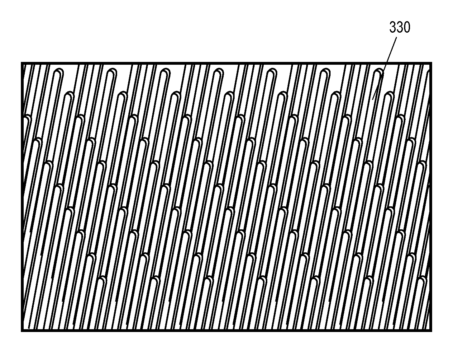
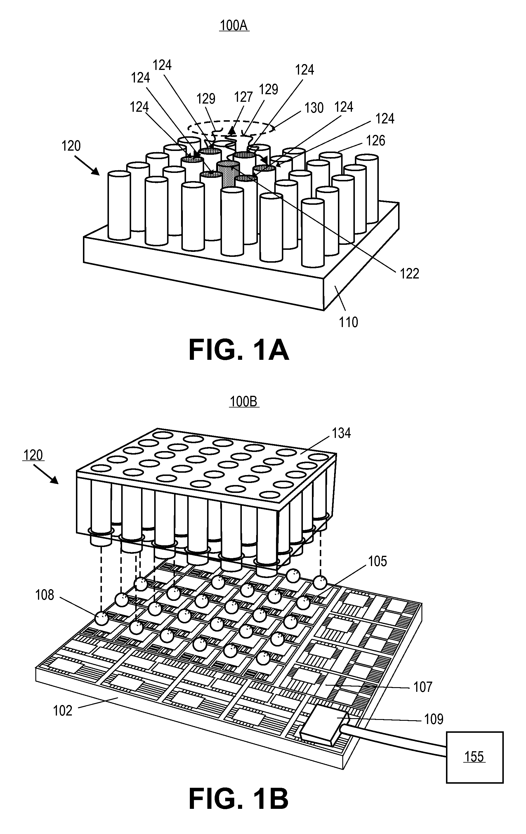
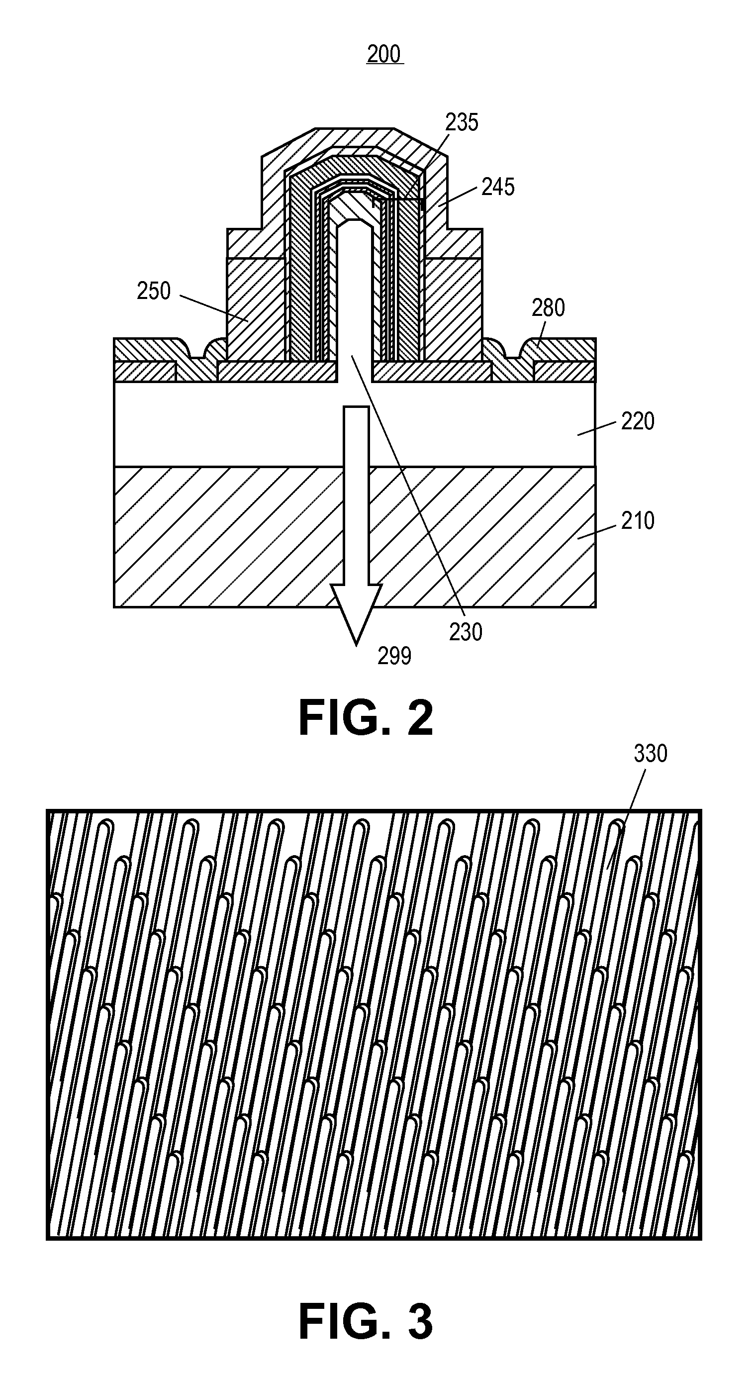
[0023]Reference will now be made in detail to exemplary embodiments of the invention, examples of which are illustrated in the accompanying drawings. Wherever possible, the same reference numbers will be used throughout the drawings to refer to the same or like parts. In the following description, reference is made to the accompanying drawings that form a part thereof, and in which is shown by way of illustration specific exemplary embodiments in which the invention may be practiced. These embodiments are described in sufficient detail to enable those skilled in the art to practice the invention and it is to be understood that other embodiments may be utilized and that changes may be made without departing from the scope of the invention. The following description is, therefore, merely exemplary.

[0024]Exemplary embodiments provide solid-state microscope devices and methods for forming and using them. The solid-state microscope devices can include a light emitter array having a plura...


PUM

PropertyMeasurementUnit
thicknessaaaaaaaaaa
thicknessaaaaaaaaaa
heightaaaaaaaaaa

Abstract

According to various embodiments, the present teachings include an array of nanowire devices. The array of nanowire devices comprises a readout integrated circuit (ROIC). An LED array is disposed on the ROIC. The LED array comprises a plurality of LED core-shell structures, with each LED core-shell structure comprising a layered shell enveloping a nanowire core, wherein the layered shell comprises a multi-quantum-well (MQW) active region. The LED array further comprises a p-side electrode enveloping the layered core-shell structure and electrically connecting the ROIC, wherein each p-side electrode has an average thickness ranging from about 100 nm to about 500 nm. A dielectric layer is disposed on the plurality of LED core-shell structures, with each nanowire core disposed through the dielectric to connect with an n-side semiconductor that is situated on the dielectric.

Description

RELATED APPLICATIONS[0001]This application is a continuation-in-part of U.S. patent application Ser. No. 12 / 880,923 entitled “Lens-less Digital Microscope,” filed Sep. 13, 2010, which claims priority from U.S. Provisional Patent Application Ser. No. 61 / 276,400, filed Sep. 11, 2009, and which is also a continuation-in-part of U.S. patent application Ser. No. 12 / 103,920, entitled “Solid State Microscope,” filed Apr. 16, 2008, which claims priority to U.S. Provisional Patent Application Ser. No. 60 / 913,927, filed Apr. 25, 2007, and Ser. No. 60 / 973,465, filed Sep. 19, 2007, all of which are hereby incorporated by reference in their entirety.GOVERNMENT RIGHTS[0002]This invention was made with government support under Contract No. EEC0812056 awarded by the National Science Foundation (NSF), and under Contract No. HR0011-05-1-0006 awarded by the Defense Advanced Research Projects Agency (DARPA). The Government has certain rights in the invention.FIELD OF THE INVENTION[0003]This invention r...

Claims


Application Information

Patent Timeline
Patent Type & Authority Patents(United States)
IPC IPC(8): H01S5/34H01S5/343H01S5/40B82Y20/00
CPCH01S5/34333H01S5/4025H01S5/34B82Y15/00G02B21/0004Y10S977/951B82Y20/00G02B21/00H01L27/156H01L33/18H01L33/24G02B21/06H01L25/167H01L2224/11
Inventor HERSEE, STEPHEN D.
Owner STC UNM
Why Eureka
Try Eureka