SiC semiconductor element

a semiconductor element and semiconductor technology, applied in the field of semiconductor elements, can solve the problems of low channel mobility, increased power consumption, low channel mobility of sic mosfets, etc., and achieve the effects of reducing threshold voltage, dramatically improving channel mobility, and reducing on-resistan

Inactive Publication Date: 2015-08-25
NARA INSTITUTE OF SCIENCE AND TECHNOLOGY
View PDF18 Cites 3 Cited by
  • Summary
  • Abstract
  • Description
  • Claims
  • Application Information

AI Technical Summary

Benefits of technology

[0045]According to the present invention, it is possible to improve the channel mobility dramatically compared to a conventionally-used crystal plane. In addition, exerting a lower threshold voltage and a characteristic of a steep rise in the drain current, if SiC-based power MOSFETs are fabricated with the crystal plane according to the present invention used as a channel, this will lead to advantageous effects of achieving a lower on-resistance and thereby a reduction in power consumption of such power devices.
[0046]Moreover, the crystal plane according to the present invention, which has a smaller number of interface defects than other crystal planes, has the advantageous effect of achieving a smaller change in temperature due to device property and therefore an improvement in the device property.

Problems solved by technology

However, it has been conventionally problematic that there are many defects in an interface between a gate insulating film (gate oxide film) and SiC and channel mobility is low in MOSFETs of SiC.
Particularly, electron mobility in a bulk crystal is as high as 800 to 1000 cm2 / Vs in 4H—SiC, whereas it has been a problem that the channel mobility (Si-face) of MOSFETs of SiC is as low as 10 cm2 / Vs.
The channel mobility of the MOSFET of SiC is low because there are many defects in the interface of SiC produced by conventional technologies, i.e. interface state density is high.
If the on-resistance value of the transistor increases, power consumption increases.
That is, by device integration, the potential of SiC originally having a high electron mobility cannot be utilized at all.

Method used


Image

  • SiC semiconductor element
  • SiC semiconductor element
  • SiC semiconductor element

Examples


embodiment 1

[Embodiment 1]

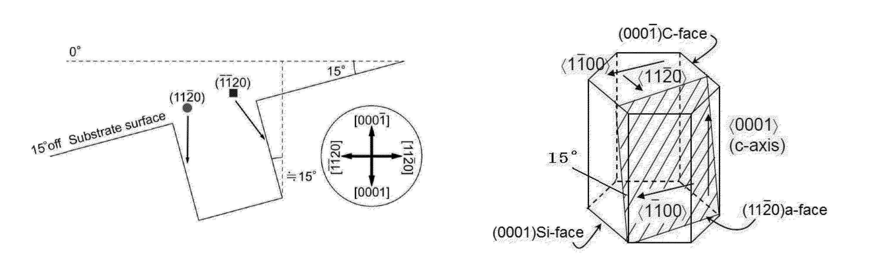
[0080]A first embodiment shows results of a device property evaluation made by fabricating a trenched MOSFET (UMOSFET) device and forming a trench having approximately vertical side walls in an SiC substrate on the (000-1) C-plane having various off-angles.

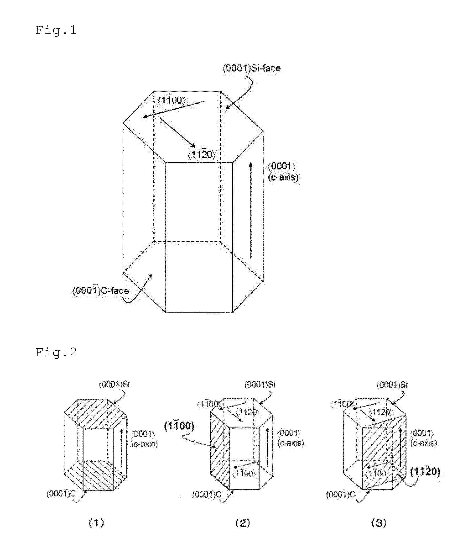
[0081]FIG. 13 schematically shows the structure of the trenched MOSFET (UMOSFET) fabricated this time. For various off-angles, the trenched MOSFET was fabricated by forming a trench having approximately vertical side walls in an SiC substrate on the (000-1) C-plane, in which the current flows in only one side of the trench side walls.

[0082]Substrates fabricated using the (000-1) plane had their respective different off-angles of 0 degrees (i.e. on-axis), 4 degrees in the [−1-120] direction, 8 degrees in the [−1-120] direction, 15 degrees in the [−1-120] direction, and 8 degrees in the [1-100] direction. The trench was formed in a rectangular shape such that adjacent side walls were at right angles to each other and t...


PUM


Abstract

The invention provides an SiC semiconductor element having fewer interface defects at the interface between the SiC and the insulating film of the SiC semiconductor, as well as improved channel mobility. The semiconductor element is provided with at least an SiC semiconductor substrate and an insulating film in contact with the substrate, wherein the insulating film is formed on a specific crystal plane of the SiC semiconductor substrate, the specific crystal plane being a plane having an off-angle of 10-20° relative to the {11-20} plane toward the [000-1] direction or at an off-angle of 70-80° relative to the (000-1) plane toward the <11-20> direction. Through the use of a specific crystal plane unknown in the prior art, interface defects between the SiC semiconductor substrate and the insulating film can be reduced, and channel mobility of the semiconductor element can be improved.

Description

TECHNICAL FIELD[0001]The present invention relates to a technology for reducing interface defects on an insulating film (oxide film) and an SiC semiconductor of an SiC semiconductor element and improving channel mobility of a MOSFET (MOS field-effect transistor) or the like.BACKGROUND ART[0002]An SiC semiconductor is a semiconductor made of SiC (silicon carbide) which is a compound of carbon (C) and silicon (Si). A most distinctive feature of the SiC semiconductor is to have a physical value suitable as a material of semiconductor devices (power devices) used in power electronics. For example, in the case of commercially available single-crystal 4H—SiC, a band gap is 3.3 eV which is three times as wide as the conventional Si semiconductor, dielectric breakdown field strength is 3 MV / cm which is about ten times as high as the conventional Si semiconductor and saturation electron velocity is three times as fast as the conventional Si semiconductor. Further, the SiC semiconductor is be...

Claims


Application Information

Patent Timeline
Patent Type & Authority Patents(United States)
IPC IPC(8): H01L29/16H01L29/78H01L29/04H01L21/04
CPCH01L29/1608H01L21/049H01L29/045H01L29/7802H01L29/7813
Inventor YANO, HIROSHIUEOKA, YOSHIHIRO
Owner NARA INSTITUTE OF SCIENCE AND TECHNOLOGY
Why Eureka
Try Eureka