Group III nitride composite substrate and method for manufacturing the same, laminated group III nitride composite substrate, and group III nitride semiconductor device and method for manufacturing the same

a technology of nitride and composite substrates, which is applied in the direction of semiconductor devices, electrical equipment, basic electric elements, etc., can solve the problems of difficulty in increasing the diameter of the substrate and decreasing the thickness, and high cost of substrate manufacturing. , to achieve the effect of small thickness variation, high crystal quality and large thickness

Inactive Publication Date: 2015-09-15
SUMITOMO ELECTRIC IND LTD
View PDF23 Cites 7 Cited by
  • Summary
  • Abstract
  • Description
  • Claims
  • Application Information

AI Technical Summary

Benefits of technology

[0013]The present invention has been made to solve the problems above and an object of the invention is to provide a low-cost and large-diameter group III nitride composite substrate including a group III nitride film having a large thickness, a small thickness variation, and a high crystal quality, a method for manufacturing the group III nitride composite substrate, a laminated group III nitride composite substrate, and a group III nitride semiconductor device and a method for manufacturing the same.
[0022]The present invention can provide a low-cost and large-diameter group III nitride composite substrate including a group III nitride film having a large thickness, a small thickness variation, and a high crystal quality, a method for manufacturing the group III nitride composite substrate, a laminated group III nitride composite substrate, and a group III nitride semiconductor device and a method for manufacturing the same.

Problems solved by technology

The free-standing group III nitride substrate disclosed in Japanese Patent Laying-Open No. 2009-126722 involves problems that the substrate is manufactured at high cost and therefore very expensive, and that the substrate is likely to crack, resulting in difficulty in increasing the diameter of the substrate and decreasing the thickness thereof.
Regarding the GaN-thin-film-bonded substrate having the GaN thin film of 0.1 μm in thickness as disclosed in Japanese Patent Laying-Open No. 2008-010766, ion implantation is performed to form the GaN thin film, which, however, involves a problem that the ion implantation degrades the crystal quality of the GaN thin film.
An increase in thickness of the GaN thin film, however, involves a problem that the variation in depth to which ions are implanted from the main surface increases, which accordingly increases the variation in thickness of the GaN thin film in the resultant GaN-thin-film-bonded substrate.
Increase of the diameter, however, involves a problem that the variation, within the main surface, of the thickness of the GaN thin film or the GaN layer increases.
In the case where a heterogeneous substrate such as sapphire substrate whose chemical composition and thermal expansion coefficient are different from those of a group III nitride substrate is prepared and a thick group III nitride film is grown on the heterogeneous substrate, there arises problems that large warp occurs and cracks are made.

Method used


Image

  • Group III nitride composite substrate and method for manufacturing the same, laminated group III nitride composite substrate, and group III nitride semiconductor device and method for manufacturing the same
  • Group III nitride composite substrate and method for manufacturing the same, laminated group III nitride composite substrate, and group III nitride semiconductor device and method for manufacturing the same
  • Group III nitride composite substrate and method for manufacturing the same, laminated group III nitride composite substrate, and group III nitride semiconductor device and method for manufacturing the same

Examples


example a

[0136]1. Fabrication of Group III Nitride Composite Substrate

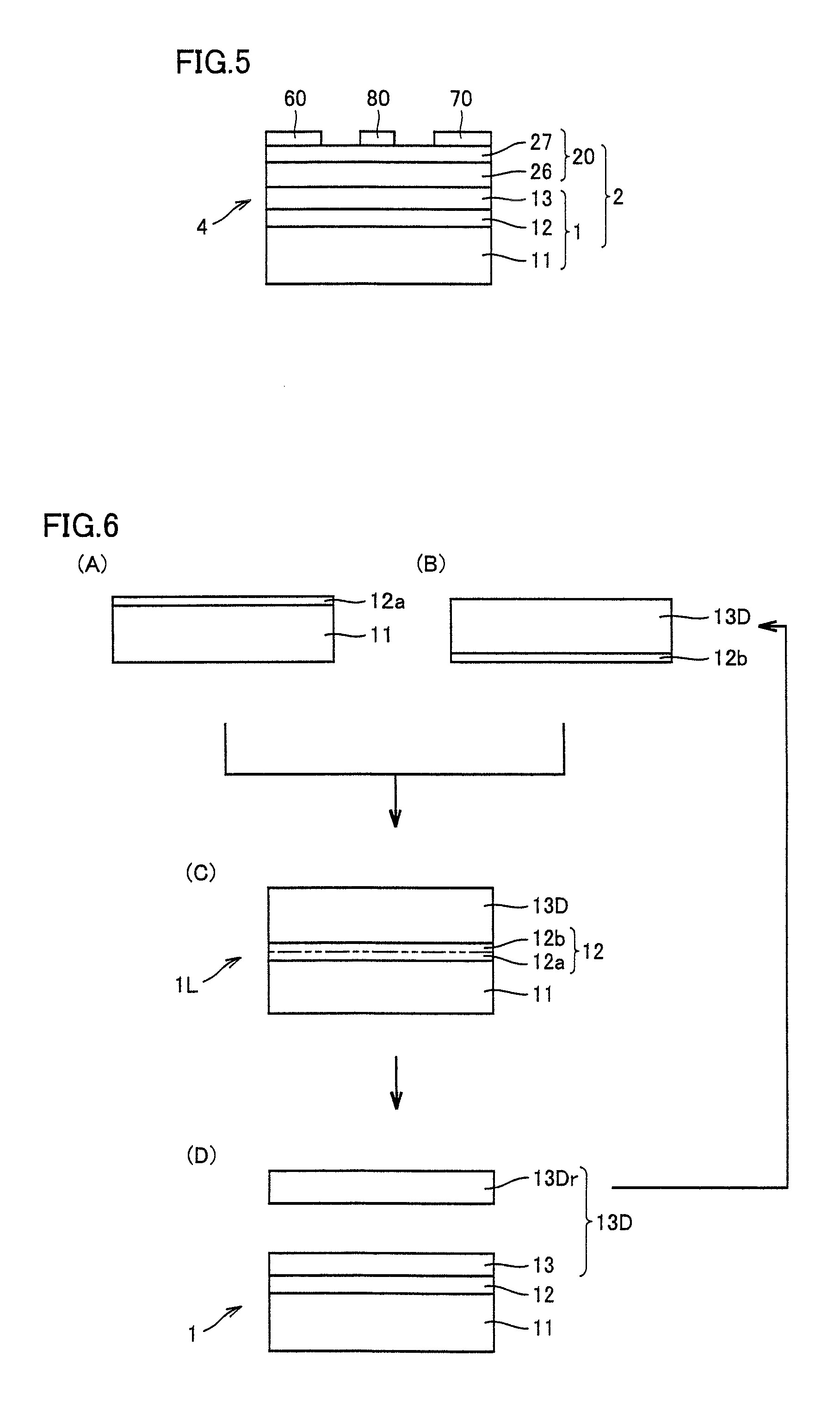
[0137]Referring to FIG. 6(A), a mullite substrate having a diameter of 75 mm was prepared for use as support substrate 11. Both surfaces of support substrate 11 were subjected to rough polishing by means of diamond abrasive grains and a copper-based surface plate, intermediate polishing by means of diamond abrasive grains and a tin surface plate, and finish polishing by means of a nonwoven polishing pad so that the surfaces were mirror-finished to have an RMS of 5 nm or less. After this, an SiO2 film was grown to a thickness of 800 nm by the LP-CVD method on at least one of these surfaces. Then, CMP was performed using a slurry having a pH of 10 and containing colloidal silica abrasive grains having an average grain size of 40 nm, to thereby form joint film 12a having a thickness of 400 nm and planarized so that the RMS of the main surface was 0.3 nm or less. In order to remove abrasive grains used for CMP, non-abrasive po...

example b

[0152]Referring to FIGS. 6 and 8, group III nitride composite substrate 1 and group III nitride semiconductor device 4 were produced in a similar manner to Example A, except that a mullite-YSZ substrate (with respect to the whole substrate, mullite was 70% by mass and YSZ was 30% by mass and, with respect to YSZ, ZrO2 was 90% by mole and Y2O3 was 10% by mole) was used as support substrate 11, and group III nitride composite substrates 1 having a diameter of 75 mm, a diameter of 100 mm, a diameter of 125 mm, and a diameter of 150 m, respectively, and having respective group III nitride films with different thicknesses as shown in Table 2 were produced.

[0153]In a similar manner to Example A, the ratio st / mt of standard deviation st of the thickness of group III nitride film 13, to mean value mt of the thickness thereof, and the ratio so / mo of standard deviation so of an absolute value of an off angle between the main surface of the group III nitride film and the (0001) plane, to mean ...

example c

[0156]As substrates for semiconductor devices, a group III nitride free-standing substrate (hereinafter also referred to as FS substrate), a group III nitride composite substrate (hereinafter also referred to as BP substrate) produced by the ion implantation method, and a group III nitride composite substrate (hereinafter also referred to as BS substrate) produced in accordance with the fourth embodiment of the present invention were prepared.

[0157]The FS substrate was prepared to have the diameter and the thickness shown in Table 3, by cutting a GaN crystal body having a predetermined diameter with a wire saw and polishing it.

[0158]The BP substrate was prepared to have the diameter and the thickness of its group III nitride film shown in Table 3. Specifically, as shown in FIG. 10(B), hydrogen ions were implanted from the main surface of the GaN crystal body having a predetermined diameter, namely group III nitride film donor substrate 13D, to the position of a predetermined depth l...


PUM

PropertyMeasurementUnit
thicknessaaaaaaaaaa
thicknessaaaaaaaaaa
diameteraaaaaaaaaa

Abstract

A group III nitride composite substrate includes a support substrate and a group III nitride film. A ratio st / mt of a standard deviation st of the thickness of the group III nitride film, to a mean value mt of the thickness thereof is 0.001 or more and 0.2 or less, and a ratio so / mo of a standard deviation so of an absolute value of an off angle between a main surface of the group III nitride film and a plane of a predetermined plane orientation, to a mean value mo of the absolute value of the off angle thereof is 0.005 or more and 0.6 or less. Accordingly, there is provided a low-cost and large-diameter group III nitride composite substrate including a group III nitride film having a large thickness, a small thickness variation, and a high crystal quality.

Description

[0001]This application claims the benefit of U.S. Provisional Application No. 61 / 712,967 filed Oct. 12, 2012, which is incorporated by reference herein in the entirety.BACKGROUND OF THE INVENTION[0002]1. Field of the Invention[0003]The present invention relates to a group III nitride composite substrate and a method for manufacturing the same, a laminated group III nitride composite substrate, and a group III nitride semiconductor device and a method for manufacturing the same.[0004]2. Description of the Background Art[0005]Group III nitrides such as GaN have superior semiconductor properties and are therefore used as materials suitable for semiconductor devices.[0006]For example, Japanese Patent Laying-Open No. 2009-126722 discloses a free-standing group III nitride substrate to be used as a substrate for a semiconductor device. The free-standing group III nitride substrate has a diameter of 25 mm or more and 160 mm or less and a thickness of 100 μm or more and 1000 μm or less. It ...

Claims


Application Information

Patent Timeline
Patent Type & Authority Patents(United States)
IPC IPC(8): H01L29/20H01L21/76H01L21/762H01L21/20H01L33/00H01L29/778
CPCH01L29/2003H01L21/2007H01L21/76254H01L29/7786H01L33/0079H01L2924/0002H01L2924/00H01L33/0093
Inventor ISHIBASHI, KEIJIHACHIGO, AKIHIROHIROMURA, YUKIMATSUMOTO, NAOKINAKAHATA, SEIJINAKANISHI, FUMITAKEYOSHIZUMI, YUSUKEMIKAMI, HIDENORI
Owner SUMITOMO ELECTRIC IND LTD
Why Eureka
Try Eureka