Organic electroluminescence device and manufacturing method thereof

a technology of electroluminescence device and manufacturing method, which is applied in the field of flat panel display, can solve the problems of reducing the yield rate insufficient activation, and deterioration of oled thin-film transistor substrate, and achieves the effect of effectively reducing the manufacturing cost and high yield ra

Inactive Publication Date: 2015-10-20
TCL CHINA STAR OPTOELECTRONICS TECH CO LTD
View PDF5 Cites 0 Cited by
  • Summary
  • Abstract
  • Description
  • Claims
  • Application Information

AI Technical Summary

Benefits of technology

[0010]An object of the present invention is to provide an organic electroluminescence device, which comprises a light absorption layer to prevent property change of a PI (Polyimide) layer during laser activation of a polysilicon layer and provide high yield rate so as to effectively reduce the manufacturing cost.
[0011]Another object of the present invention is to provide a manufacturing method of an organic electroluminescence device, which arranges a light absorption layer between an organic substrate layer and a buffer layer to prevent the organic substrate layer from changing property due to absorption of laser in a laser activation process of a polysilicon layer so as to improve the yield rate of the organic electroluminescence device and reduce the manufacturing cost.
[0016]wherein the light absorption layer absorbs the laser that transmits through the active thin-film transistor pixel array and irradiates the light absorption layer during the laser annealing in order to prevent the organic backing layer from being affected by the laser and getting deteriorated.
[0023]The organic electroluminescence device further comprises a buffer layer, the buffer layer being arranged between the light absorption layer and the active thin-film transistor pixel array to prevent impurities from spreading to the active thin-film transistor pixel array.
[0058]The efficacy of the present invention is that the present invention provides an organic electroluminescence device and a manufacturing method thereof, wherein a light absorption layer is arranged between an organic backing layer and a buffer layer in order to effectively prevent the organic backing layer from changing property resulting from absorption of laser during a laser activation process of a polysilicon layer and increase the yield rate of the organic electroluminescence device. Further, the manufacturing process is simple and the cost is low so as to be advantageous for cost control.

Problems solved by technology

When the high temperature activation is employed, due to the presence of a PI (Polyimide) layer, the activation temperature is not allowed to exceed 400° C. However, if the temperature is lower than 400° C., insufficiency of activation may result, leading to deterioration of the OLED thin-film transistor substrate.
When laser activation is employed, irradiation of the laser to the PI layer causes property change of the PI layer due to absorption of the laser, leading to lowering of the yield rate of the OLED thin-film transistor substrate and increasing of the manufacturing cost.

Method used


Image

  • Organic electroluminescence device and manufacturing method thereof
  • Organic electroluminescence device and manufacturing method thereof
  • Organic electroluminescence device and manufacturing method thereof

Examples


Embodiment Construction

[0065]To further expound the technical solution adopted in the present invention and the advantages thereof, a detailed description is given to a preferred embodiment of the present invention and the attached drawings.

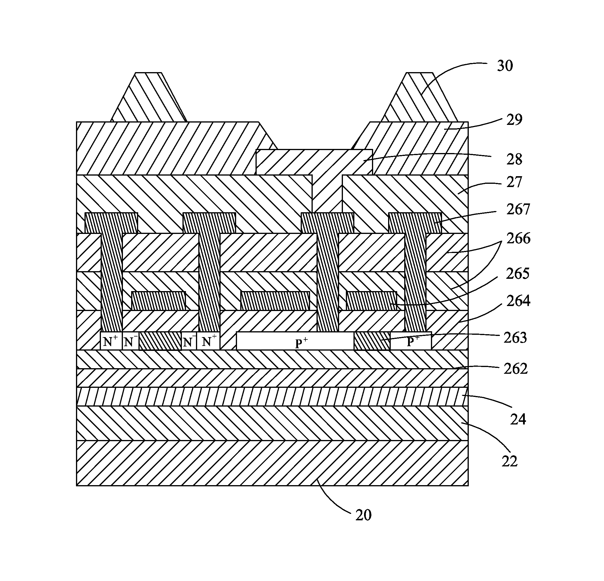
[0066]Referring to FIG. 3, the present invention provides an organic electroluminescence device. The organic electroluminescence device is formed on a substrate 20 and comprises: an organic backing layer 22, which provides a flexible base and isolates external moisture; a light absorption layer 24, which is arranged on the organic backing layer 22; an active thin-film transistor pixel array, which is arranged on the light absorption layer 24, the active thin-film transistor pixel array comprising at least a crystalline semiconductor layer that is formed by means of laser annealing; and an organic electroluminescence layer 29, which is arranged on the active thin-film transistor pixel array. The light absorption layer 24 absorbs the laser that transmits through the acti...


PUM


Abstract

The present invention provides an organic electroluminescence device and a manufacturing method thereof. The organic electroluminescence device includes: an organic backing layer (22), which provides a flexible base and isolates external moisture; a light absorption layer (24), which is arranged on the organic backing layer (22); an active thin-film transistor pixel array, which is arranged on the light absorption layer (24), the active thin-film transistor pixel array comprising at least a crystalline semiconductor layer that is formed by means of laser annealing; and an organic electroluminescence layer (29), which is arranged on the active thin-film transistor pixel array. The light absorption layer (24) absorbs the laser that transmits through the active thin-film transistor pixel array and irradiates the light absorption layer (24) during the laser annealing in order to prevent the organic backing layer (22) from being affected by the laser and getting deteriorated.

Description

BACKGROUND OF THE INVENTION[0001]1. Field of the Invention[0002]The present invention relates to the field of flat panel displaying, and in particular to an organic electroluminescence device and a manufacturing method thereof.[0003]2. The Related Arts[0004]A flat display device has various advantages, such as thin device body, low power consumption, and being free of radiation, and is thus of wide applications. The flat display devices that are currently available include liquid crystal displays (LCDs) and organic electroluminescence devices (OELDs), which are also referred to as organic light emitting diodes (OLEDs).[0005]The known liquid crystal displays are generally backlighting liquid crystal displays, which include an enclosure, a liquid crystal display panel arranged in the enclosure, and a backlight module mounted inside the enclosure. The principle of operation of the liquid crystal display panel is that liquid crystal molecules are interposed between two parallel glass su...

Claims


Application Information

Patent Timeline
Patent Type & Authority Patents(United States)
IPC IPC(8): H01L29/08H01L29/51H01L23/522H01L51/56H01L29/167H01L29/45H01L29/49H01L29/66H01L29/16H01L51/50H01L29/786H01L29/04H01L27/32H01L51/00H01L35/24H01L51/52
CPCH01L27/3258H01L23/5226H01L27/3248H01L27/3262H01L29/04H01L29/16H01L29/167H01L29/458H01L29/495H01L29/4908H01L29/51H01L29/518H01L29/66757H01L29/78603H01L29/78675H01L51/0015H01L51/0027H01L51/0097H01L51/5012H01L51/5253H01L51/5259H01L51/5284H01L51/56H01L51/0034H01L2227/323H01L2251/301H01L2251/308H01L2251/5338H01L27/1218H01L27/1274H01L2924/0002H01L29/78633Y02E10/549Y02P70/50H10K59/1213H10K50/865H10K2102/311H01L2924/00H10K59/124H10K50/11H10K50/844H10K50/846H10K59/123H10K71/00H10K71/211H10K71/421H10K77/111H10K59/1201H10K85/10H10K2102/00H10K2102/103
Inventor HSU, YUANJUN
Owner TCL CHINA STAR OPTOELECTRONICS TECH CO LTD
Why Eureka
Try Eureka