Blankmask and method for fabricating photomask using the same

a technology which is applied in the field blank mask and method for fabricating photomask using the same, can solve the problems of increasing the time for increasing the thickness of resist film, and increasing the cost of etching hard mask film, so as to achieve sufficient process margin and improve the critical dimension (cd) features

Active Publication Date: 2016-01-05
S & S TECH
View PDF14 Cites 3 Cited by
  • Summary
  • Abstract
  • Description
  • Claims
  • Application Information

AI Technical Summary

Benefits of technology

[0012]The present invention is directed to a blankmask in which a light-shielding layer is formed to a thin thickness so as to form a high-resolution pattern (e.g., a pattern of 32 nm or less) that has pattern fidelity corresponding to the resolution thereof, chemical resistance, and a sufficient process margin for defect repair, and that has improved critical dimension (CD) features, such as precise CD mean-to-target (MTT) matching a high resolution, CD uniformity, and CD linearity, and a photomask using the blankmask.
[0013]The present invention is also directed to a blankmask in which a hard mask film is formed of a new material capable of decreasing an etch rate thereof to form a resist film as a thin film, thereby enabling formation of a high-resolution pattern, and a photomask using the blankmask.

Problems solved by technology

Today, as the increasingly high integration density of large-scale integrated circuits (ICs) has been accompanied by the need for ever finer circuit patterns, semiconductor microfabrication process technology has emerged as a very important issue.
However, the following problems may occur when such a fine pattern is formed using a conventional blankmask for a hardmask.
A first problem is related to the thickness of the resist film.
However, when a material of a conventional hard mask film is used to form a high-resolution pattern, the time for etching the hard mask film becomes relatively long.
Thus, it is difficult to form the resist film as a thin film.
Even if a new material can be used instead, it is actually difficult to select a material that has not only selectivity (dry etch characteristics) with respect to the light-shielding layer below the resist film but also a least CD bias with respect to the light-shielding layer.
A second problem is related to pattern fidelity according to the thickness of the light-shielding layer.
However, since the light-shielding layer should have not only light-shielding properties (optical density) capable of blocking incident light, but also chemical resistance, exposure resistance, a sufficient defect repair margin, etc., the light-shielding layer is very difficult to form as a thin film.

Method used


Image

  • Blankmask and method for fabricating photomask using the same
  • Blankmask and method for fabricating photomask using the same
  • Blankmask and method for fabricating photomask using the same

Examples


examples

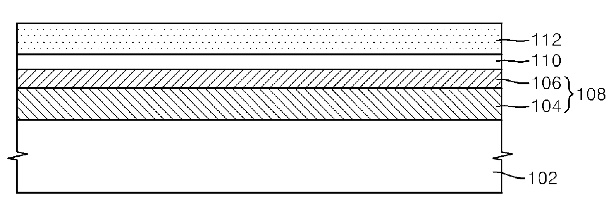
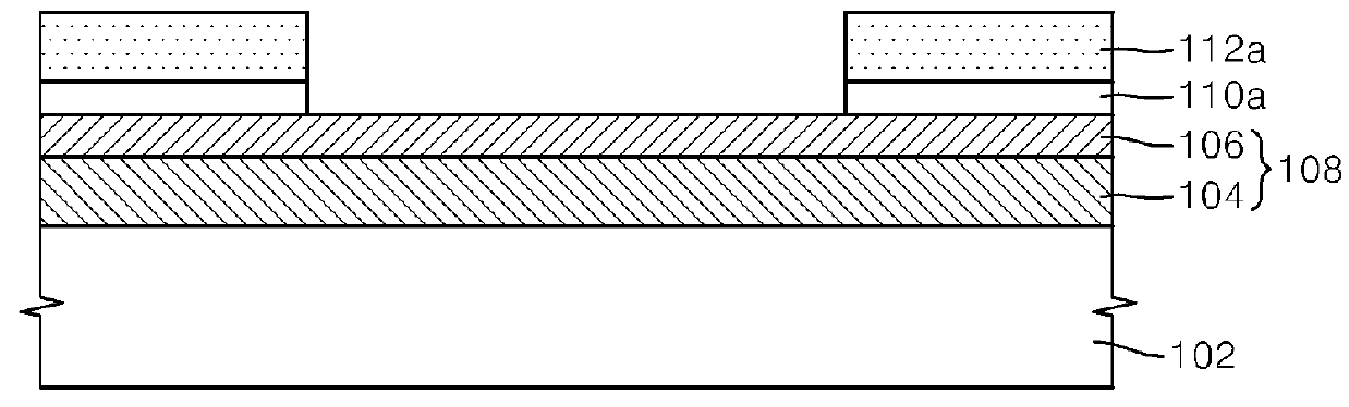
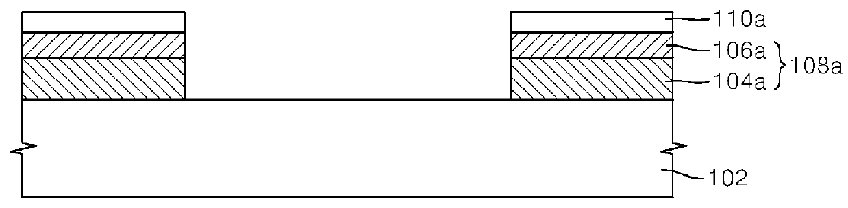
[0058]Method of Manufacturing a Blankmask for a Hardmask

[0059]In the blankmask 100 for a hardmask, the light-shielding layer 108 and the hard mask film 110 were formed using a DC magnetron reactive sputtering device. A sputtering process was performed using at least one gas selected from the group consisting of argon (Ar), nitrogen (N), nitrogen monoxide (NO), carbon dioxide (CO2), methane (CH4), helium (He), and nitrogen dioxide (NO2).

[0060]First, the light-shielding layer 108 having a two-layer structure including the light block layer 104 and the anti-reflective layer 106 was formed on the transparent substrate 102 formed of synthetic quartz glass having a size of 6025 (6×6×0.25 inches). Specifically, the light block layer 104 formed of MoTaSiN was formed on the transparent substrate 102 by performing a film forming process with process power of 0.6 kW for 250 seconds by using a MoTaSi target (Mo:Ta:Si=20 at %:30 at %:50 at %) as a sputtering target and a process gas having a com...


PUM

PropertyMeasurementUnit
surface reflectivityaaaaaaaaaa
optical densityaaaaaaaaaa
flatnessaaaaaaaaaa

Abstract

Provided is a blankmask with a light-shielding layer including a light block layer and an anti-reflective layer, and a hard mask film. The light block layer and the anti-reflective layer are formed by combining a layer formed of a MoSi compound and a layer formed of a MoTaSi compound. Thus, the blankmask enables formation of a pattern of 32 nm or less, since the light-shielding layer can be thinly formed to a thickness of 200 to 700 and a photomask having pattern fidelity corresponding to the resolution of the pattern can be formed. The light-shielding layer has an optical density of 2.0 to 4.0 at an exposure wavelength of 193 nm, chemical resistance, and a sufficient process margin for defect repair. Further, the hard mask film is formed to a thickness of 20 to 50 using a compound including tin (Sn) and chromium (Cr), thereby decreasing an etch rate of the hard mask film. Accordingly, a resist film can be formed as a thin film, thereby manufacturing a high-resolution blankmask.

Description

CROSS-REFERENCE TO RELATED APPLICATION[0001]This application claims priority to and the benefit of Korean Patent Application No. 2012-0070772, filed on Jun. 29, 2012, the disclosure of which is incorporated herein by reference in its entirety.BACKGROUND[0002]1. Field of the Invention[0003]The present invention relates to a blankmask and method for fabricating a photomask using the same, and more particularly, to a blankmask that can be formed to have a resolution of 32 nm or less and that has a pattern fidelity corresponding to the resolution, and a method of fabricating a photomask using the same.[0004]2. Discussion of Related Art[0005]Today, as the increasingly high integration density of large-scale integrated circuits (ICs) has been accompanied by the need for ever finer circuit patterns, semiconductor microfabrication process technology has emerged as a very important issue. In the case of a highly integrated circuit, circuit wires become finer for low power consumption and hig...

Claims


Application Information

Patent Timeline
Patent Type & Authority Patents(United States)
IPC IPC(8): G03F1/50
CPCG03F1/50G03F1/24G03F1/00G03F1/80
Inventor NAM, KEE-SOOKANG, GEUNG-WONYANG, CHUL-KYULEE, JONG-HWAJANG, KYU-JIN
Owner S & S TECH
Why Eureka
Try Eureka