Method for manufacturing laminated coil devices

a technology of laminated coils and manufacturing methods, which is applied in the manufacture of coils, fixed inductances, and inductances, etc., can solve the problems of parallely-connected coils exponentially increasing the cost of products, difficult to form narrow and thick electrodes, and difficult to form thin thin electrodes. , to achieve the effect of reducing impedance and inductance value, reducing cost, and controlling electrode width

Active Publication Date: 2016-02-02
SHENZHEN SUNLORD ELECTRONICS
View PDF13 Cites 0 Cited by
  • Summary
  • Abstract
  • Description
  • Claims
  • Application Information

AI Technical Summary

Benefits of technology

[0010]A main object of the present invention is to provide a method of manufacture that produces a laminated coil power device with low thickness and low direct current resistance.
[0023]According to the above mentioned method of the present invention, because the coil conductors will not spread, and thereby the width of the electrode is controlled. Furthermore, there is unlikely a reduction of the area surrounding the coils causing a decrease of impedance and inductance value. On the other hand, the electrode does not project and interfere with the connection between layers, eliminating the possibility of an air space that might result in short circuit of the electrode, lamination cracking, and delamination for the present invention.
[0024]Generally speaking, according to the method of the present invention, it provides a convenient, low cost method of manufacturing narrow and thick coil electrodes, but also provides the ability for small, thin low cost manufacture of laminated coil power device with large impedance and inductance value, low DC resistance, low in cost, small in size, and low thickness.

Problems solved by technology

In the traditional method, after the electrode paste is printed on the insulating layer 202, the electrode paste inevitably spreads out in a manner that makes it difficult to form a narrow and thick electrode.
Thus the traditional laminated coil device may be characterized by a mismatch of the ceramic insulating layers 202 involving air spaces 203, which may short circuit the electrode, and result in lamination cracking, and delamination.
However, although the parallely-connected coils are able to reduce the impedance and inductance value of the product, the multiple parallely-connected coils exponentially increase the cost of the products, and have the limitation of a reduction of thickness.
Although this, on one hand, dramatically increases the length of the magnetic path and decreases the impedance and inductance value of the products, on the other hand, this method is high in cost, and has the limitation of thinning.

Method used


Image

  • Method for manufacturing laminated coil devices
  • Method for manufacturing laminated coil devices
  • Method for manufacturing laminated coil devices

Examples


first embodiment

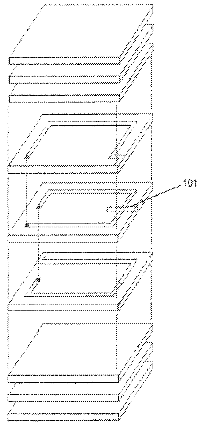
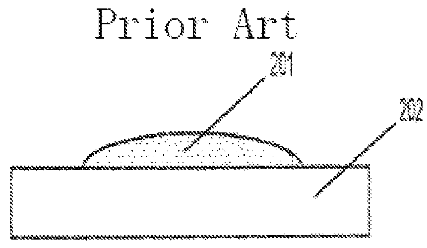
[0050]In general, in order to obtain the laminated coil device having large impedance, large inductance value, and low direct current resistance, the design of the electrode coil has to meet explicit requirements. FIG. 5 shows the top perspective view of the laminated bodies, and the ratio of the thickness and width of the electrode fillers must be larger than 20%. the width of the electrode 501 is designed as 235 um, and that is the ratio of the thickness and width of the electrode is 21.3%. Before sintering, the distance between the outer margin of the electrode and the outer margin of the laminated bodies 502 must be less than 120 um. In the first preferred embodiment, the distance between the outer margin of the electrode and the outer margin of the laminated bodies 502 is 100 um. In other words, before sintering, an area 503 surrounding by the coil is up to 30% percentage of the surface area of the laminated bodies.

[0051]The laminated bodies are heated at the temperature of 40...

second embodiment

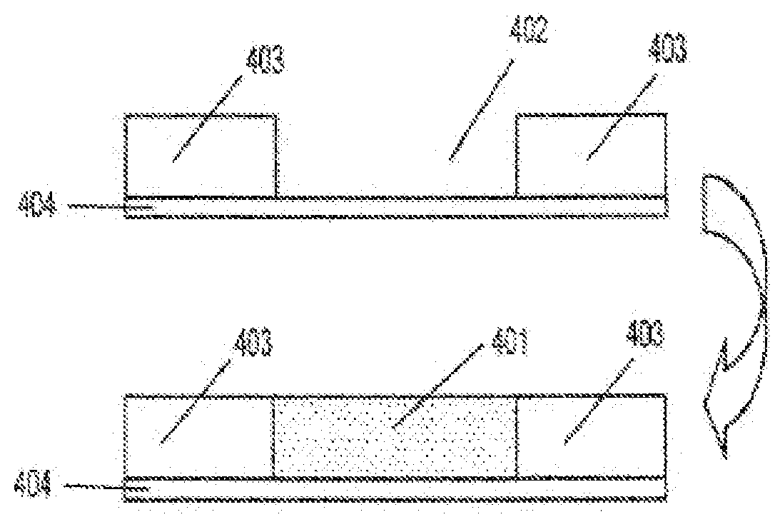
[0055]After drying, the depth of the trenches is equal to the thickness of the main part of the coil thin sheets 403. In the second embodiment, the depth of the trenches 402 defined as 50 um is equal to the thickness of the main part of the coil thin sheets 403. By the screen printing method, the conductive paste primarily including silver is printed into the coil-shaped trenches 402 so as to form coil electrode 401. The thickness of the conductive paste is either equal or slightly larger than the depth of the coil-shaped trenches 402. In the second preferred embodiment of the present invention, the thickness of the fillers defined as 50 um is equal to the depth of the coil-shaped trenches 402. Depending on the existing of through holes, the conductive paste is also able to fill into the through holes in order to reach the connection between each coil conductors after stacking. It is worth mentioning that the lowermost main part of the coil thin sheets 403 and electrode 401 do not n...


PUM

PropertyMeasurementUnit
temperatureaaaaaaaaaa

Abstract

A method of manufacturing a laminated coil device includes conductors for forming coils and insulation stacking for forming laminated bodies, and further includes the steps of: (A) manufacturing ceramic insulating thin sheets; (B) forming ceramic insulating thin sheets with conductive through-holes; (C) manufacturing coil thin sheets with coil conductors so as to embed the coil conductors inside the ceramic insulating thin sheets; (D) orderly stacking and cutting ceramic insulating thin sheets and coil thin sheets with coil conductors into unit sizes in order to obtain laminated bodies; (E) heating the laminated bodies in order to remove the binder, and then sintering the laminated bodies; (F) coating the conductive paste on the two ends of the laminated bodies so as to form external electrodes. Thus, the present invention is to provide a manufacturing method of producing a laminated coil power device with low direct current resistance, no delamination, no air space, and no lamination cracking.

Description

NOTICE OF COPYRIGHT[0001]A portion of the disclosure of this patent document contains material which is subject to copyright protection. The copyright owner has no objection to any reproduction by anyone of the patent disclosure, as it appears in the United States Patent and Trademark Office patent files or records, but otherwise reserves all copyright rights whatsoever.BACKGROUND OF THE PRESENT INVENTION[0002]1. Field of Invention[0003]The present invention relates to a method of manufacturing a laminated coil device.[0004]2. Description of Related Arts[0005]A laminated coil power device can be one of laminated large-current ferrite chip beads, a laminated power inductor, and a laminated power transformer. Laminated coil devices are widely applied to the power cable of many kinds of portable products because it has the advantages of high reliability, may be mass produced, and is easily miniaturized and thinned.[0006]Particularly, when the laminated coil power device uses ceramic ma...

Claims


Application Information

Patent Timeline
Patent Type & Authority Patents(United States)
IPC IPC(8): H01F7/06H01F41/04H01F17/00
CPCH01F41/04H01F17/0013H01F41/042Y10T29/4902
Inventor LI, YOUYUNLU, DAFUZHANG, YANGYUAN, CONG
Owner SHENZHEN SUNLORD ELECTRONICS
Why Eureka
Try Eureka