
Composite substrate for light emitting diodes

a technology of light-emitting diodes and composite substrates, which is applied in the direction of circuit optical details, printed circuit aspects, and non-printed circuit optical details, etc., can solve the problems of excessive cost of using highly reflective aluminum substrates as an entire surface of led luminaires, degraded performance and operational life of led dies, and light-emitting does not occur, etc., to achieve superior reflectivity and heat conductivity.

Active Publication Date: 2016-02-02
SIGNIFY HLDG BV
View PDF8 Cites 18 Cited by
  • Summary
  • Abstract
  • Description
  • Claims
  • Application Information

AI Technical Summary

Benefits of technology

The patent describes a device for packaging LED dies that provide better reflectivity and heat conduction without using expensive, highly reflective substrates. It includes a highly reflective substrate that is placed in a hole in a printed circuit board. The LED dies are mounted directly on the substrate. The printed circuit board has a layer of glass fiber in resin and a metal layer. The substrate is thermally coupled to a heat sink using a thermal interface material. The metal layer of the printed circuit board is electrically coupled to the LED dies through bond wires, and no electrical connection is made to any LED die on the top surface of the substrate. This device provides superior performance at a lower cost.

Problems solved by technology

Some of the emitted light does not, however, exit the LED package because the light is absorbed by surfaces of the package.
The performance and operational lifetime of the LED dies is degraded if the operating temperature exceeds a threshold level.
Although the chip-on-board packaging 10 does exhibit the two desired LED packaging qualities of effective heat dissipation and high reflectivity, the cost of using the highly reflective aluminum substrate as an entire surface of the LED luminaire is exceedingly expensive.

Method used


Image

  • Composite substrate for light emitting diodes
  • Composite substrate for light emitting diodes
  • Composite substrate for light emitting diodes

Examples


Embodiment Construction

[0026]Reference will now be made in detail to some embodiments of the invention, examples of which are illustrated in the accompanying drawings.

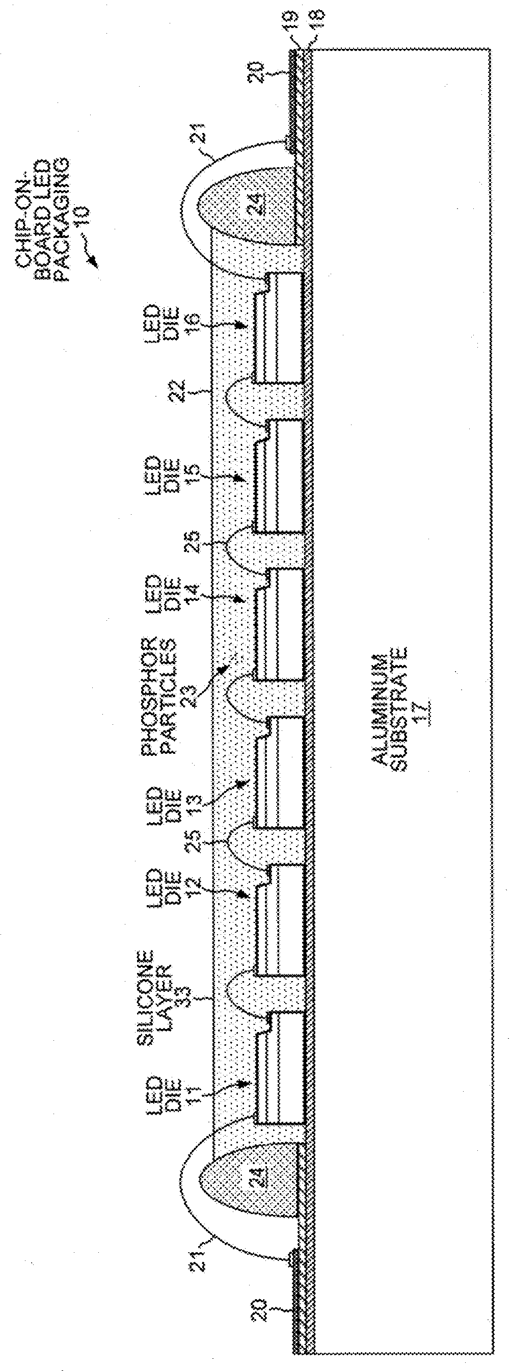
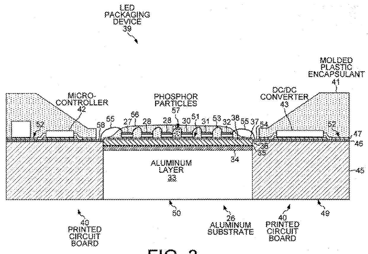
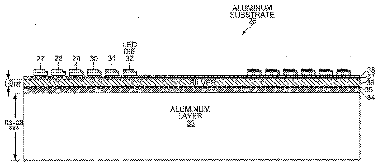
[0027]FIG. 2 shows a highly reflective aluminum substrate 26 onto which light emitting diodes (LEDs) 27-32 have been mounted in a chip-on-board (COB) manner. The LED dies 27-32 are placed directly onto the substrate 26 in the die-bonding process. In one implementation, gold bond wires link the LED dies 27-32 in series, and the ends of the series-connected strings of LED dies are wire bonded to conductive traces deposited on the top surface of the aluminum substrate. In one embodiment, the top surface of the aluminum substrate is an insulating layer. The aluminum substrate 26 itself performs the functions of light reflection and heat dissipation. A luminaire made with the COB aluminum substrate 26 can be placed directly on a heat sink without any intervening printed circuit board layer. In another embodiment, substrate 26 has a base layer mad...


PUM


Abstract

A low-cost device for packaging LED dies provides superior reflectivity and thermal conductivity without covering entire surfaces of an LED luminaire with an expensive reflective aluminum substrate. The LED packaging device includes a highly reflective substrate disposed in a hole in a printed circuit board. The substrate has a reflectivity greater than 97% and includes an insulating layer and a reflective layer disposed above a thicker aluminum layer. An LED die is disposed on the top surface of the substrate. The PCB has a layer of glass fiber in resin and a metal layer. The lower surface of the PCB and the bottom surface of the substrate are substantially coplanar. The metal layer of the PCB is electrically coupled to the LED die only through bond wires. Electronic circuitry is disposed on the upper surface of the PCB and is used to control light emitted from the LED die.

Description

TECHNICAL FIELD[0001]The present invention relates generally to packaging for light-emitting diodes, and more particularly, to a composite substrate that maintains high reflectivity and thermal conductivity at lower cost.BACKGROUND INFORMATION[0002]A light emitting diode (LED) is a solid state device that converts electrical energy to light. Light is emitted from active layers of semiconductor material sandwiched between oppositely doped layers when a voltage is applied across the doped layers. Multiple LED dies are typically packages together in an LED array. In one example, an array of LED dies is mounted onto a heat conducting substrate, and a layer of silicone is disposed over the LED dies. When a current is driven through the LED dies, the dies emit blue light. Some of the blue light emitted from the LED dies is absorbed by phosphor particles embedded in the silicone and is re-emitted by the phosphor particles as longer wavelength light. The combined light emitted by the LED di...

Claims


Application Information

Patent Timeline
Patent Type & Authority Patents(United States)
IPC IPC(8): H01L27/15H01L29/88H01L33/20H01L33/58H05K1/02H05K1/18H01L25/16H01L33/60H01L33/48H01L33/50H01L33/64H01L33/56H01L33/62
CPCH01L33/20H01L33/486H01L33/502H01L33/644H01L33/56H01L33/62H01L33/60H01L25/167H01L25/165H05K1/181H05K1/0274H01L33/58H05K2201/10106H05K2201/10166H05K2201/0275H01L25/0753H01L2924/181H01L2224/48091H01L2224/48137H01L2224/49107H01L2224/49109H01L2224/8592H01L2224/73265H05K1/184H05K2201/10643H05K2203/049H01L33/50H01L2924/00012H01L2924/00014H01L33/507
Inventor CUMPSTON, BRIAN
Owner SIGNIFY HLDG BV
Features
  • Generate Ideas
  • Intellectual Property
  • Life Sciences
  • Materials
  • Tech Scout
  • Unparalleled Data Quality
  • Higher Quality Content
  • 60% Fewer Hallucinations
Learn More