Method for forming an electrically conductive oxide film, an electrically conductive oxide film, and uses for the same

a technology of electrically conductive oxide and oxide film, which is applied in the direction of oxide conductors, non-metal conductors, superimposed coating processes, etc., can solve the problems of poor uniformity and homogeneity of coating poor electrically conductive oxide films that have not been demonstrated using ald, and poor ability to uniformly and homogeneously coat non-planar surfaces and substrates with complex shapes. , to achieve accura

Active Publication Date: 2016-03-22
BENEQ OY
View PDF20 Cites 3 Cited by
  • Summary
  • Abstract
  • Description
  • Claims
  • Application Information

AI Technical Summary

Benefits of technology

[0023]According to one embodiment of the present invention the method comprises forming an electrically conductive, light absorbing oxide film. According to one embodiment of the present invention the method comprises forming a lossy film. The method of the present invention results in a film with very conformal coverage even over complex non-planar surfaces of 3D objects. Among other benefits, this facilitates e.g. the optical design of coatings employing this film. The material of the film exhibits good chemical stability when exposed to e.g. atmospheric conditions or to other potentially oxidizing conditions in which the film may be exposed to moisture and / or oxygen. The method of the present invention enables the fabrication of an electrically conductive oxide film. The fabrication method for the film furthermore enables accurate control of the electrical conductivity of the film. The material of the film surprisingly also exhibits a high absorption coefficient and, for some embodiments of the present invention, relatively uniform absorption spectra in the visible part of the electromagnetic spectrum.
[0025]An electrically conductive film of this oxide can be formed by alternately repeating the steps of forming the preliminary deposit and treating the formed deposit. This electrically conductive oxide film possesses the advantageous properties discussed above. Furthermore, the alternate growth of the preliminary deposit and the treating of this deposit leads to an at least partly self-limiting growth mechanism which results in the advantageous conformality of the electrically conductive oxide film with a relatively uniform thickness profile.
[0029]As each exposure of the surface of the substrate to a chemical results in a portion of the chemical being adsorbed onto the surface of the substrate, the number of how many times the surface of the substrate is exposed to the chemicals can be utilized in some embodiments of the invention to control the thickness of the film. These methods of forming a film on a substrate therefore enable very accurately controlling the thickness of the film. Hence, the total absorption of light in the film, and therefore the darkness of the film, can be accurately controlled. When the chemicals responsible for film growth are alternately present in the reaction space the chemicals are not able to significantly intermix and the growth of the highly absorbing film is predominantly governed by adsorption reactions on the deposition surface. The kinetics of these adsorption reactions are, on the other hand, governed predominantly by the properties of the deposition surface and not so much by the flow dynamics of the chemicals over the deposition surface and in the reaction space. In some embodiments of the invention this results in the highly absorbing film being very conformal and having a very uniform thickness essentially regardless of the shape of the substrate (or of the deposition surface).
[0030]In one embodiment of the invention the steps a), b), and c) are each carried out one or more times for forming a film having a thickness between 1 nm to 2 μm on the substrate. When the thickness of the film is below 1 nm or above 2 μm the film is essentially transparent or opaque, respectively, to human eye. Therefore films falling within the range of 1 nm to 2 μm can be efficiently used as greyscale filters.
[0036]By suitably choosing the chemicals and the process parameters, especially the temperature of the substrate when the surface of the substrate is exposed to chemicals and the pressure inside the reaction space, the adsorption of chemicals onto the deposition surface, the growth of the preliminary deposit of transition metal oxide and the treatment of this preliminary deposit with the organometallic chemical, can be made essentially self-limiting. This further improves the thickness uniformity of the resulting film and conformality on the surface of 3D objects with complex shapes. Additionally many of the chemicals listed above are inexpensive and the method of the invention can be carried out cost-effectively.

Problems solved by technology

But, dark colored light-absorbing oxide films being electrically conductive have not been demonstrated using ALD.
A problem with these coating methods is their poor ability to uniformly and homogeneously coat non-planar surfaces and substrates with complex shapes.
This is especially detrimental in decorative applications where the coating is intended to provide a specific appearance uniformly over the entire surface of the substrate.
The methods for depositing chromium oxide are not able to produce films with uniform thickness and uniform optical properties over non-planar surfaces of e.g. three dimensional (3D) objects with complex shapes.
Chromium and chromium oxide materials also have further drawbacks related to the allergenic properties of chromium.

Method used


Image

  • Method for forming an electrically conductive oxide film, an electrically conductive oxide film, and uses for the same
  • Method for forming an electrically conductive oxide film, an electrically conductive oxide film, and uses for the same
  • Method for forming an electrically conductive oxide film, an electrically conductive oxide film, and uses for the same

Examples


example 1

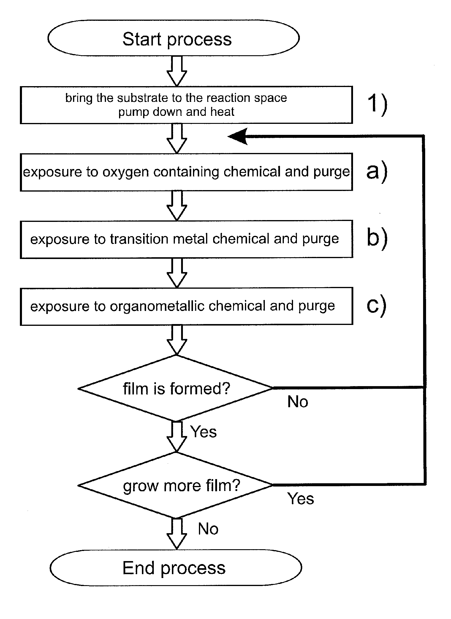
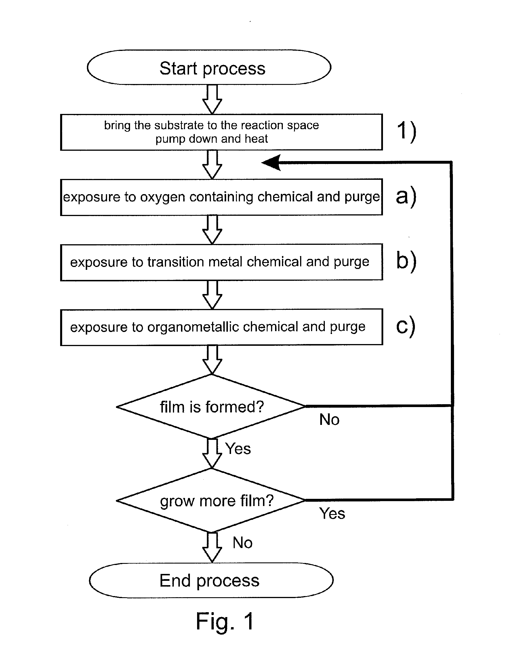
[0066]According to the first embodiment of the invention (see FIG. 1) electrically conductive oxide films were formed on substrates using different processing temperatures. Visibly essentially transparent D263T glass substrates with a thickness of 0.3 mm (available from Schott AG, Germany) were first inserted inside the reaction space of a P400 ALD batch tool (available from Beneq OY, Finland). The substrates were planar to enable e.g. reliable optical transmission measurements. The substrates were positioned inside the reaction space such that the bottom side of the substrate glass was masked to enable film growth only on the top side, which was exposed to the surrounding reaction space. In this example the carrier gas discussed above and responsible for purging the reaction space was nitrogen (N2).

[0067]After preparations for loading the substrates into the ALD tool, the reaction space of the ALD tool was pumped down to underpressure and a continuous flow of carrier gas was set to...

example 2

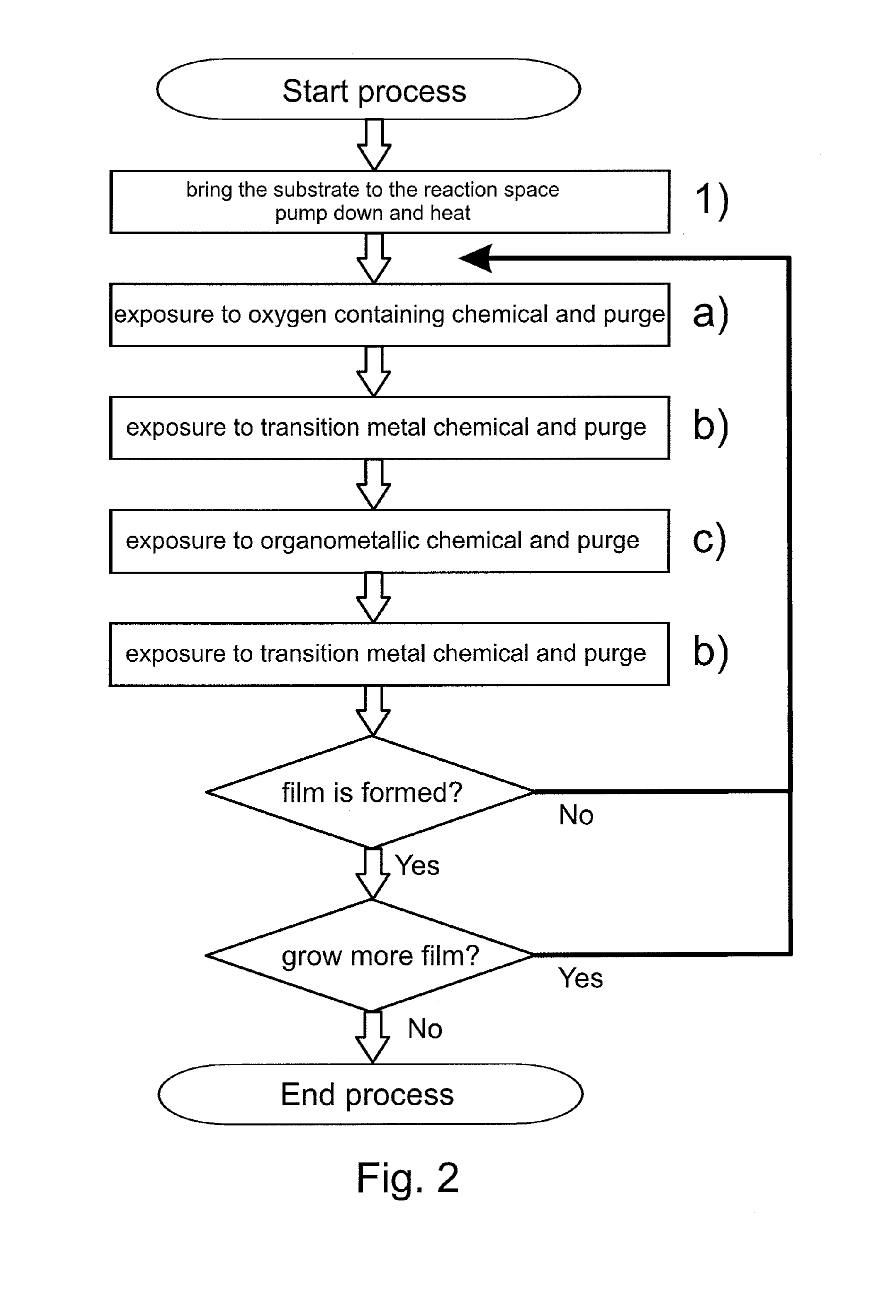
[0076]Electrically conductive oxide films were formed on substrates according to the second embodiment of the invention (see FIG. 2). Visibly essentially transparent D263T glass substrates with a thickness of 0.3 mm (available from Schott AG, Germany) were first inserted inside the reaction space of a P400 ALD batch tool (available from Beneq OY, Finland). The substrates were planar to enable reliable optical transmission measurements. The substrates were positioned inside the reaction space such that one side of the substrate glass was exposed (i.e. the other side of the substrate glass was masked) to the surrounding reaction space. In this example the carrier gas discussed above and responsible for purging the reaction space was nitrogen (N2).

[0077]After preparations for loading the substrates into the ALD tool, the reaction space of the ALD tool was pumped down to underpressure and a continuous flow of carrier gas was set to achieve the processing pressure of about 1 mbar (1 hPa)...

example 3

[0085]FIG. 6 presents transmission data obtained from an electrically conductive oxide film formed according to the first embodiment of the invention (sample 191 of FIG. 6). This electrically conductive oxide film was formed at a processing temperature of 280° C. with the procedure identical to example 1, with the exception that the sequence a), then b), then c) was carried out once and then repeated 1999 times.

[0086]As can be inferred from FIG. 6 the film exhibit relatively uniform optical absorption in the visible part of 400-750 nm of the electromagnetic spectrum.

[0087]Although the adsorption reactions responsible for film growth in this example are not completely understood, test runs indicated that the chemical adsorption reactions were self-limiting to at least some extent. This resulted in very conformal and uniform films over large areas of the surface and even over complex non-planar surfaces.

[0088]Further, the thickness of the film formed was about 220 nm (using the above ...


PUM

PropertyMeasurementUnit
thicknessaaaaaaaaaa
pressureaaaaaaaaaa
pressureaaaaaaaaaa

Abstract

A method for forming an electrically conductive oxide film (1) on a substrate (2), the method comprising the steps of, bringing the substrate (2) into a reaction space, forming a preliminary deposit on a deposition surface of the substrate (2) and treating the deposition surface with a chemical. The step of forming the preliminary deposit on the deposition surface of the substrate (2) comprises forming a preliminary deposit of transition metal oxide on the deposition surface and subsequently purging the reaction space. The step of treating the deposition surface with a chemical comprises treating the deposition surface with an organometallic chemical and subsequently purging the reaction space, to form oxide comprising oxygen, first metal and transition metal. The steps of forming the preliminary deposit and treating the deposition surface being alternately repeated such that a film (1) of electrically conductive oxide is formed on the substrate (2).

Description

[0001]This application is a National Stage Application of PCT / FI2010 / 050874, filed 2 Nov. 2010, which claims benefit of Serial No. 20096154, filed 6 Nov. 2009 in Finland and which applications are incorporated herein by reference. To the extent appropriate, a claim of priority is made to each of the above disclosed applications.FIELD OF THE INVENTION[0002]The present invention relates to film deposition technology. Especially the present invention relates to a method for forming an electrically conductive, light absorbing oxide film by forming a deposit on a deposition surface and treating this deposit with a chemical, and to electrically conductive, light absorbing oxide films fabricated using such a method.BACKGROUND OF THE INVENTION[0003]Atomic Layer Deposition (ALD) is a well known method for depositing conformal thin-films with relatively uniform thickness profile over substrates of various shapes, even over complex 3D (three dimensional) structures. In ALD the coating is grown...

Claims


Application Information

Patent Timeline
Patent Type & Authority Patents(United States)
IPC IPC(8): H01B1/02C23C30/00C23C28/00C23C16/455C23C16/44C23C16/40C23C16/08C23C16/18
CPCC23C16/18C23C16/40C23C16/403C23C16/405C23C16/4408C23C16/45523C23C16/08C23C28/00C23C30/00H01B1/08C23C16/45525C23C16/45531C23C28/04
Inventor MAULA, JARMO
Owner BENEQ OY
Why Eureka
Try Eureka