Phase noise reduction in voltage controlled oscillators

a voltage control and phase noise technology, applied in oscillator generators, instruments, computing, etc., to achieve the effect of reducing noise contribution and maintaining stable oscillator outpu

Active Publication Date: 2016-05-03
IBM CORP
View PDF19 Cites 13 Cited by
  • Summary
  • Abstract
  • Description
  • Claims
  • Application Information

AI Technical Summary

Benefits of technology

[0006]In one embodiment, the VCO comprises an LC tank circuit for generating an oscillator output signal at an oscillator frequency (fo), and an oscillator core including first and second cross-coupled semiconductor devices connected to the tank circuit to provide regenerative feedback to the tank circuit to help maintain the oscillator output stable. The VCO further comprises a supply node connected to the tank circuit and to the oscillator core for connecting the VCO to a voltage source, a tail node connected to the tank circuit and to the oscillator core for connecting the VCO to a current source, and a noise by-pass circuit. The noise by-pass circuit is connected to the supply node and to the tail node, in parallel with the LC tank circuit and the oscillator core, and forms a low-impedance path at a frequency approximately twice the oscillator frequency to at least partially immunize the oscillator core from external noise and to reduce noise contribution from the cross-coupled semiconductor devices.
[0016]In one embodiment, the invention provides a method of designing a voltage controlled oscillator comprising an LC tank circuit for generating an oscillator output, an oscillator core to provide regenerative feedback to the tank circuit, supply and tail nodes, and a noise by-pass circuit. The method comprises designing the oscillator core to generate the oscillator output at a frequency of fo, biasing the core, and connecting the core to a voltage supply; designing the noise by-pass circuit at approximately twice the frequency of the oscillator output; and introducing the noise by-pass circuit into the VCO. The noise by-pass circuit is connected to the supply node and to the tail node, in parallel with the LC tank circuit and the oscillator core, to at least partially immunize the oscillator core from external noise and to reduce noise contribution from the oscillator core. The method further comprises tuning the noise by-pass circuit to obtain a specified performance of the VCO.
[0021]In one embodiment, the invention provides a design structure tangibly embodied in a machine readable medium for design, manufacturing, or testing a semiconductor device. The design structure comprises a semiconductor substrate including a voltage controlled oscillator (VCO). The VCO comprises an LC tank circuit for generating an oscillator output signal at an oscillator frequency (fo), and an oscillator core including first and second cross-coupled semiconductor devices connected to the tank circuit to provide regenerative feedback to the tank circuit to help maintain the oscillator output stable. The VCO further comprises a supply node connected to the tank circuit and to the oscillator core for connecting the VCO to a voltage source, a tail node connected to the tank circuit and to the oscillator core for connecting the VCO to a current source, and a noise by-pass circuit. The noise by-pass circuit is connected to the supply node and to the tail node, in parallel with the LC tank circuit and the oscillator core, and forms a low-impedance path at a frequency approximately twice the oscillator frequency to at least partially immunize the oscillator core from external noise and to reduce noise contribution from the cross-coupled semiconductor devices.

Problems solved by technology

This phase noise, which varies over time, may be due to the thermal noise present in the components of the oscillator, loss in the passive components, and to other factors.

Method used


Image

  • Phase noise reduction in voltage controlled oscillators
  • Phase noise reduction in voltage controlled oscillators
  • Phase noise reduction in voltage controlled oscillators

Examples


embodiment 220

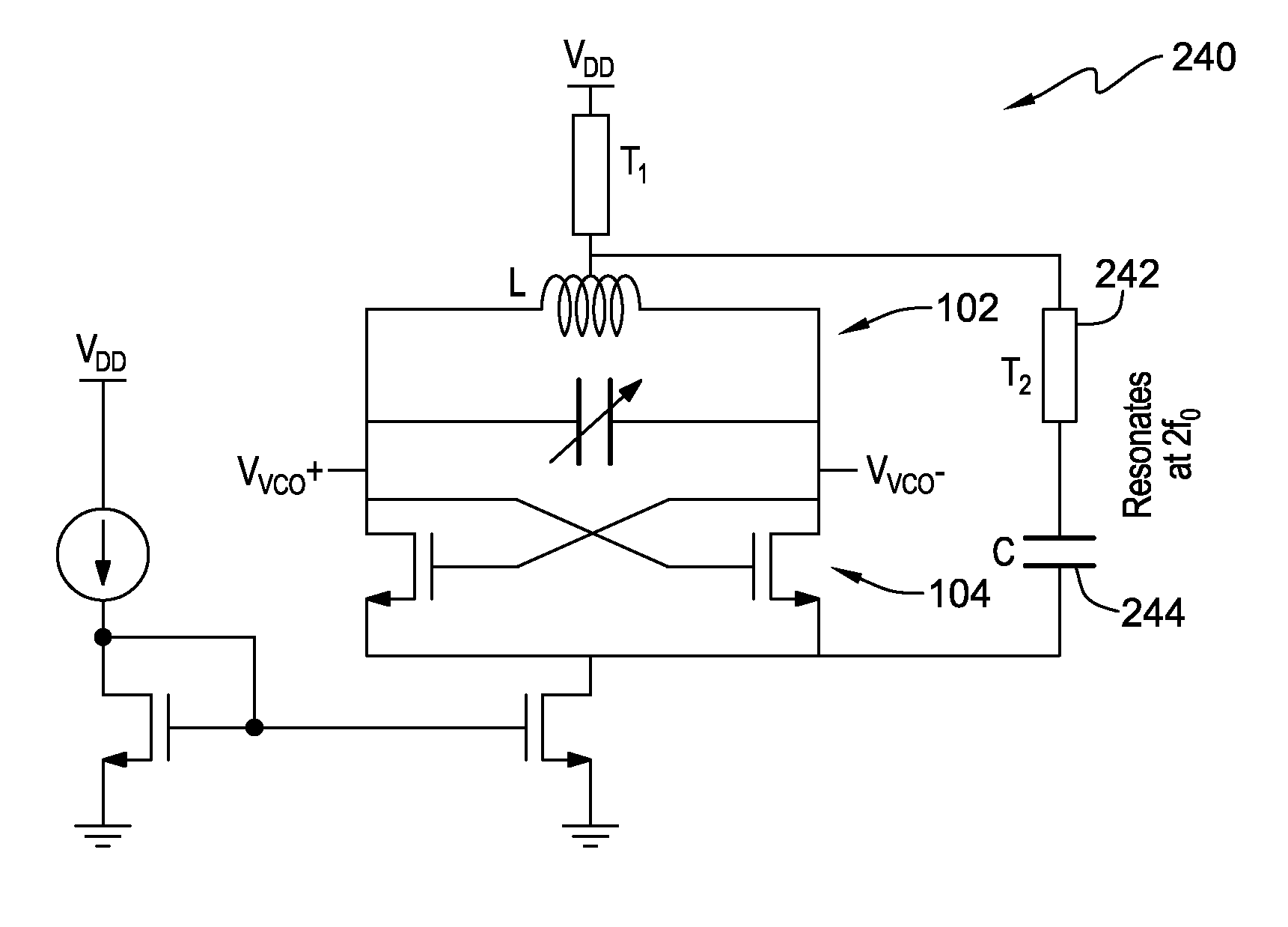
[0065]FIG. 6 shows an alternate embodiment 220 of this invention, in which an inductor 222 is added in series with capacitor 224. The inductor 222 and capacitor 224 are tuned to resonate at twice the frequency of the oscillator (2fosc), forming a low-impedance path at that frequency. Because the impedance seen towards this noise bypass circuit (formed by inductor 222 and 224) is lower than that seen towards the VCO core, the noise from the tail current source at 2fosc that flows into the VCO is reduced significantly. In embodiments of the invention, the design of FIG. 6, in comparison with the design of FIG. 5, uses smaller components. For instance, in the architecture of FIG. 6, a 100 pH t-line and a 250 fF capacitor 224 may be used. As an example: Simulated phase noise for 37 GHz oscillator: −126.6 dBc / Hz (as good as C 204 of FIG. 5)

[0066]In a simulation, the circuit of FIG. 6 also reduced noise from the cross-coupled transistor pair; and in some cases, the short at 2fosc, of FIG....

embodiment 300

[0070]With the embodiment 300 of FIG. 8, capacitor 302 is a variable capacitor. A first voltage control V1 304 is shown applied to capacitor 110, and second voltage control V2 306 is applied to capacitor 302. The voltage control V2 is used to control the capacitor 302 such that T2 310 and the capacitor resonate at approximately 2fosc, with adjustments thereto to improve or optimize the overall performance of the oscillator.

[0071]With the arrangement 320 shown in FIG. 9, digital control set O2 322 is applied to transmission line T2 324. The control is used to set the inductance of the transmission line so that T2 and capacitor 326 resonate at approximately 2fosc, with adjustments thereto to improve or optimize the overall performance of the oscillator. With this embodiment, as illustrated in FIG. 9, capacitor 326 does not need to be a variable capacitor.

[0072]The circuit 340 of FIG. 10 includes both a variable capacitor 342 and a variable inductance transmission line T2 344. Voltage ...


PUM


Abstract

A voltage controlled oscillator (VCO), a method of designing a voltage controlled oscillator, and a design structure comprising a semiconductor substrate including a voltage controlled oscillator are disclosed. In one embodiment, the VCO comprises an LC tank circuit for generating an oscillator output at an oscillator frequency, and an oscillator core including cross-coupled semiconductor devices to provide feedback to the tank circuit. The VCO further comprises a supply node, a tail node, and a noise by-pass circuit connected to the supply and tail nodes, in parallel with the tank circuit and the oscillator core. The by-pass circuit forms a low-impedance path at a frequency approximately twice the oscillator frequency to at least partially immunize the oscillator core from external noise and to reduce noise contribution from the cross-coupled semiconductor devices.

Description

STATEMENT OF GOVERNMENT INTEREST[0001]This invention was made with Government support under Contract No.: FA8650-09-C-7924 (Defense Advanced Research Projects Agency (DARPA)). The Government has certain rights in this invention.BACKGROUND[0002]This invention generally relates to voltage controlled oscillators, and more specifically, to reducing noise in such oscillators.[0003]In general, a VCO (voltage controlled oscillator) is an oscillator circuit that outputs an AC signal having a frequency that varies in response to an input control voltage. VCOs are fundamental components that are employed in a broad range of applications including radar and communications systems (e.g., wireline or wireless applications) for data transfer and recovery processes. By way of example, VCOs are utilized for PLL (phase locked loop) circuits, DLL (delay locked loop) circuits, and injection locked oscillators. VCOs are further employed for applications such as frequency translation, data modulation, c...

Claims


Application Information

Patent Timeline
Patent Type & Authority Patents(United States)
IPC IPC(8): H03B5/08G06F17/50H03B1/00H03B5/12
CPCG06F17/5045G06F17/5063H03B1/00H03B5/1215H03B5/1228H03B5/1243H03B5/1281H03B2200/009H03B2200/0038G06F30/36G06F30/30G06F30/327H03B5/1212
Inventor VALDES-GARCIA, ALBERTOSADHU, BODHISATWA
Owner IBM CORP
Why Eureka
Try Eureka