Composite substrates for acoustic wave elements, and acoustic wave elements
a technology substrates, applied in the field of acoustic wave elements, can solve the problems of reducing the thickness of the propagation substrate, deteriorating the propagation efficiency of surface acoustic waves, and reducing the q value in the case of surface acoustic wave filters, so as to reduce the temperature coefficient of frequency change, reduce the effect of expansion and contraction, and improve the propagation efficiency of acoustic waves
- Summary
- Abstract
- Description
- Claims
- Application Information
AI Technical Summary
Benefits of technology
Problems solved by technology
Method used
Image
Examples
example 1
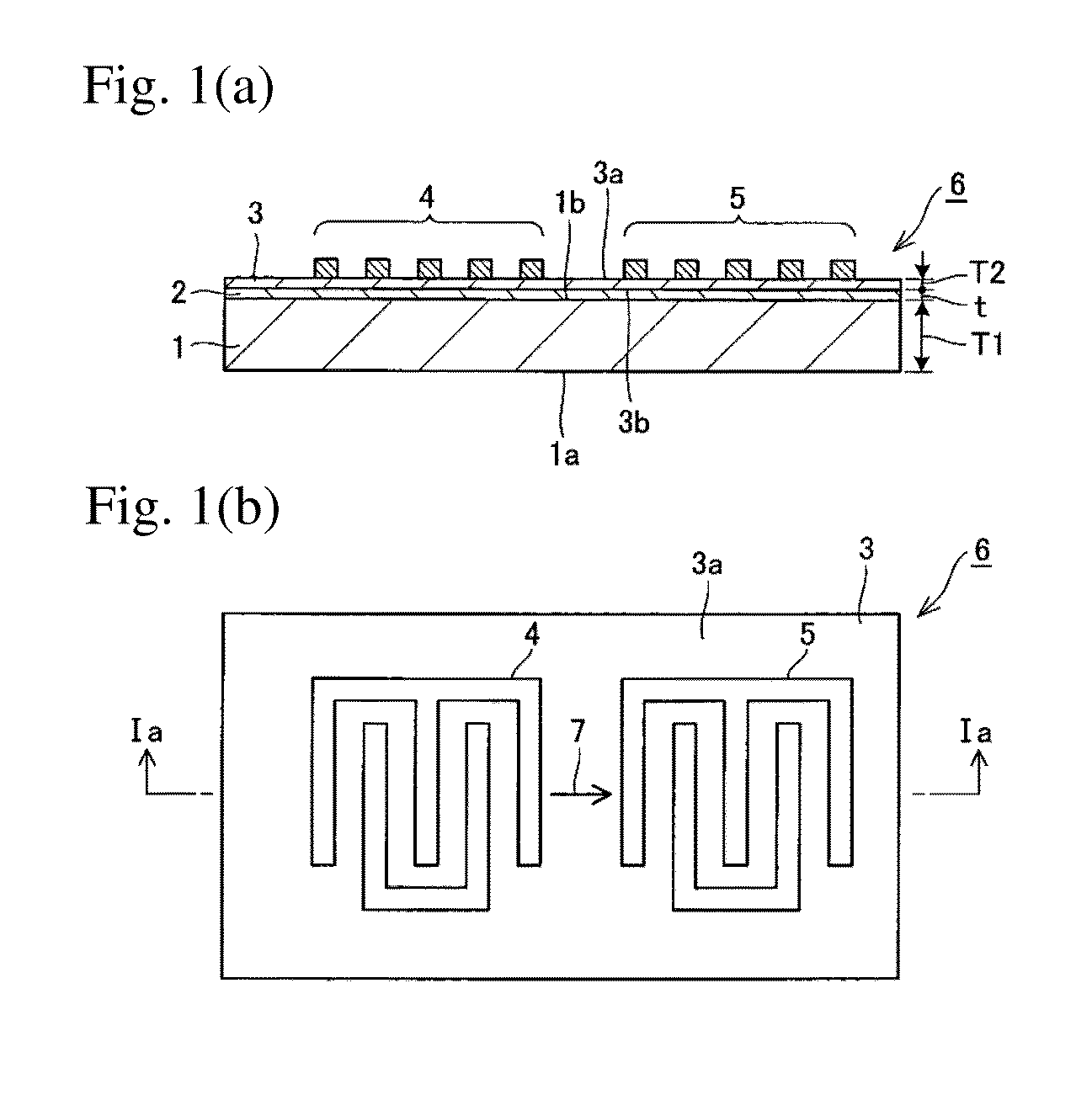
[0069]A surface acoustic wave element 6A as shown in FIG. 1(b) and FIG. 3(a) was manufactured according to the manufacturing method shown in FIGS. 6 and 7.
[0070]As the support substrate 1, a single-crystal silicon substrate of 230 μm in thickness and 4 inches in diameter was used. The linear expansion coefficient in SAW-propagating direction X of the support substrate 1 is 3 ppm / ° C. As the propagation substrate material 3A, a 36° Y-cut, X-propagation lithium tantalate substrate having SAW-propagating direction of X and a rotary Y-cut cutting angle was used. The linear expansion coefficient in the SAW-propagating direction X is 16 ppm / ° C. The thickness of the propagation substrate material 3A was 230 μm.
[0071]The support substrate and the propagation substrate material were introduced into a vacuum chamber keeping a vacuum of 10−6 Pa digits, and held therein with the respective bonding faces being opposed to each other. The bonding face of the support substrate and the bonding face...
example 2
[0079]In the example 1 described above, instead of the urethane foam pad, a harder pad of non-woven cloth was used to perform the polishing for the finishing. It was taken a photograph by TEM in the vicinity of the surface of the thus obtained propagation substrate to prove that the thickness of the lattice distortion layer was 8 nm. Further, the three layers, having different contrasts, were observed in the surface region as the Example 1.
[0080]A metal aluminum-made input electrode 4 and output electrode 5 of 0.14 μm in thickness were formed on this propagation substrate. The ratio of electrode thickness t / elastic surface wave wavelength λ was 7%. The frequency temperature characteristics (Temperature Coefficient of Frequency) of the resulting surface acoustic wave element was as good as −13 ppm / ° C. as measured at the resonance point thereof. The insertion loss was, however, proved to be 8 dB, which was lower. It is considered that the surface distortion layer is thicker and the a...
example 3
[0081]A bonded substrate was produced in the same manner as Example 1. However, instead of the above-mentioned silicon substrate, a sapphire substrate having the same thickness as the silicon substrate was used, as the support substrate. The frequency temperature characteristics at the resonance point were −18 ppm / ° C. in this case.
PUM
 Abstract
Description
Claims
Application Information


