

Reading device and method for measuring energy and flight time using silicon photomultipliers
a technology of reading device and flight time, which is applied in the direction of measuring device, scientific instruments, instruments, etc., can solve the problems of compromising the targeted time resolution and the strict limits of the detector on power consumption, so as to reduce the amount of data to be processed by the chip backend, the effect of good timing accuracy and low speed
- Summary
- Abstract
- Description
- Claims
- Application Information
AI Technical Summary
Benefits of technology
Problems solved by technology
Method used
Image

Examples
Embodiment Construction
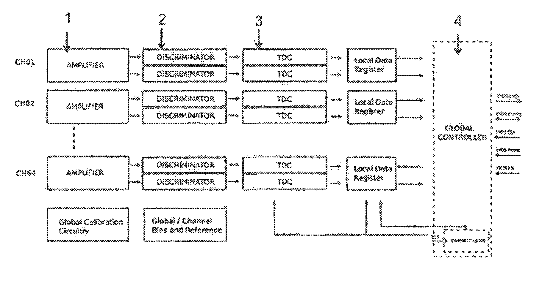
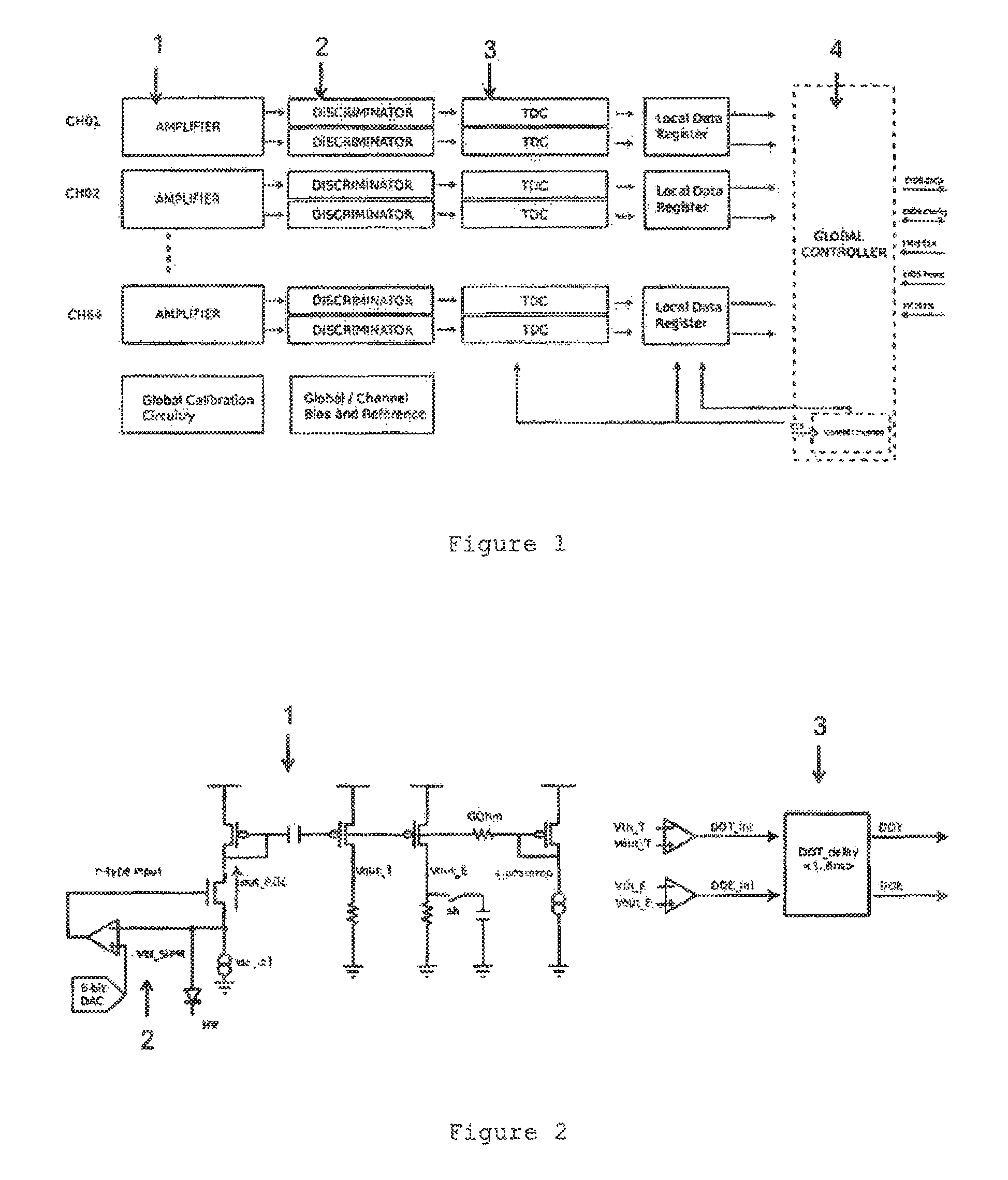
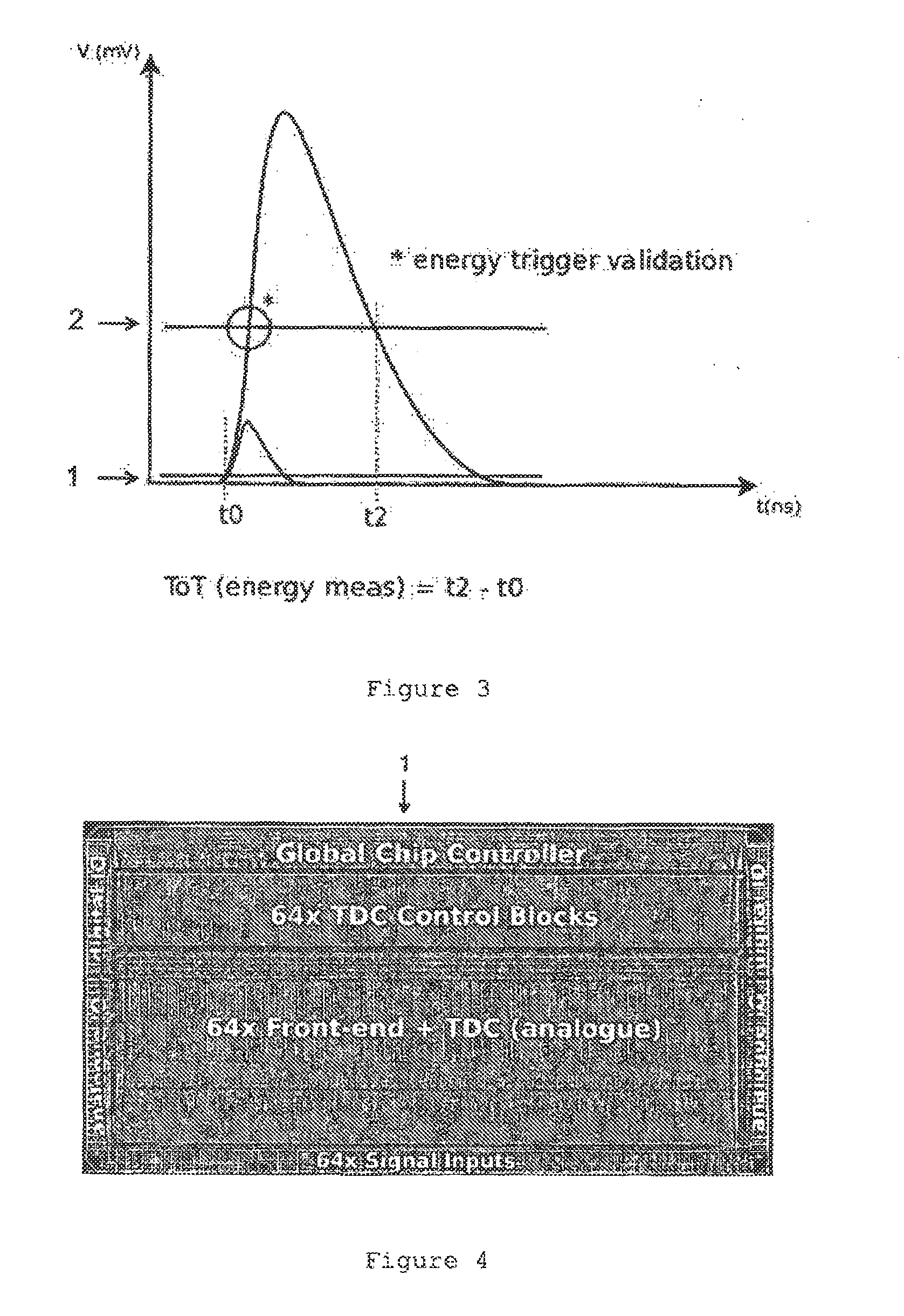
[0027]The present invention, described below with a preferred embodiment, refers to a readout apparatus for time-of-flight and energy measurements characterized by using silicon photomultipliers (SiPM), providing accurate time-of-flight information when used in PET systems with fast crystals (e.g. LYSO), which allow to confine the origin of the two 511 keV photons with a position uncertainty of 30 mm along the line-of-response (LOR) and permit unprecedented PET sensitivity.
[0028]The preferred embodiment of the readout architecture described is an ASIC made up of 64 channels, bias and calibration blocks and a global controller. One edge is free of pins, such that a twin chip rotated by 180° can be abutted to build a compact 128 channel circuit (cf. FIG. 4). Nominal operation mode uses a 160 MHz clock generated off-chip. Up to two LVDS data output links are available (SDR or DDR), for a total bandwidth from 160 to 640 Mbit / s.
[0029]An output clock for synchronous transmission is availa...
PUM
 Abstract
Description
Claims
Application Information