High-frequency power supply device

a power supply device and high-frequency technology, applied in the direction of optical radiation measurement, instruments, spectrophotometry/monochromators, etc., can solve the problems of difficult control of dc bias voltage, poor efficiency of amplifier elements using vacuum tubes, and failure of semiconductor devices, so as to improve the efficiency of cooling efficiency, facilitate the flow of air into the device, and prevent the effect of air pollution of the parts inside the devi

Active Publication Date: 2016-12-20
SHIMADZU CORP
View PDF17 Cites 0 Cited by
  • Summary
  • Abstract
  • Description
  • Claims
  • Application Information

AI Technical Summary

Benefits of technology

[0015]The present invention has been made in view of the above circumstances, and has its aim to provide a highly reliable and highly efficient high-frequency power supply device with a simple circuit configuration which is capable of preventing pollution of parts inside the device by air outside the device, where there is no need to supply a DC bias voltage to control terminals of a semiconductor device according to an increase in a feedback voltage.
[0028]According to the present invention, the wiring between the input terminal and the output terminal of the secondary coil of the transformer and the control terminals of the semiconductor device may be made short, and the coupling coefficient between the primary coil and the secondary coil is increased, and thus the feedback voltage may be increased. Also, according to the present invention, air outside the device can be prevented from easily flowing into the device, and pollution of the parts inside the device by the air outside the device may be prevented.

Problems solved by technology

However, an amplifier element using a vacuum tube is not only poor in efficiency, but also requires periodic replacement due to short life and due to a change over time in electrical characteristics being great.
However, variation or fluctuation in the electrical characteristics of a semiconductor device, such as the amplification factor and an input threshold voltage, is great, and it is difficult to control the DC bias voltage to be an optimum value at all times. Also, if the DC bias voltage becomes too high, a large current flows due to the semiconductor device being placed in a complete on state, and the semiconductor device may be broken.
Moreover, the semiconductor device on the high side has to be a DC bias circuit not connected to ground potential, and there is a problem that the cost is increased.

Method used


Image

  • High-frequency power supply device
  • High-frequency power supply device
  • High-frequency power supply device

Examples


Embodiment Construction

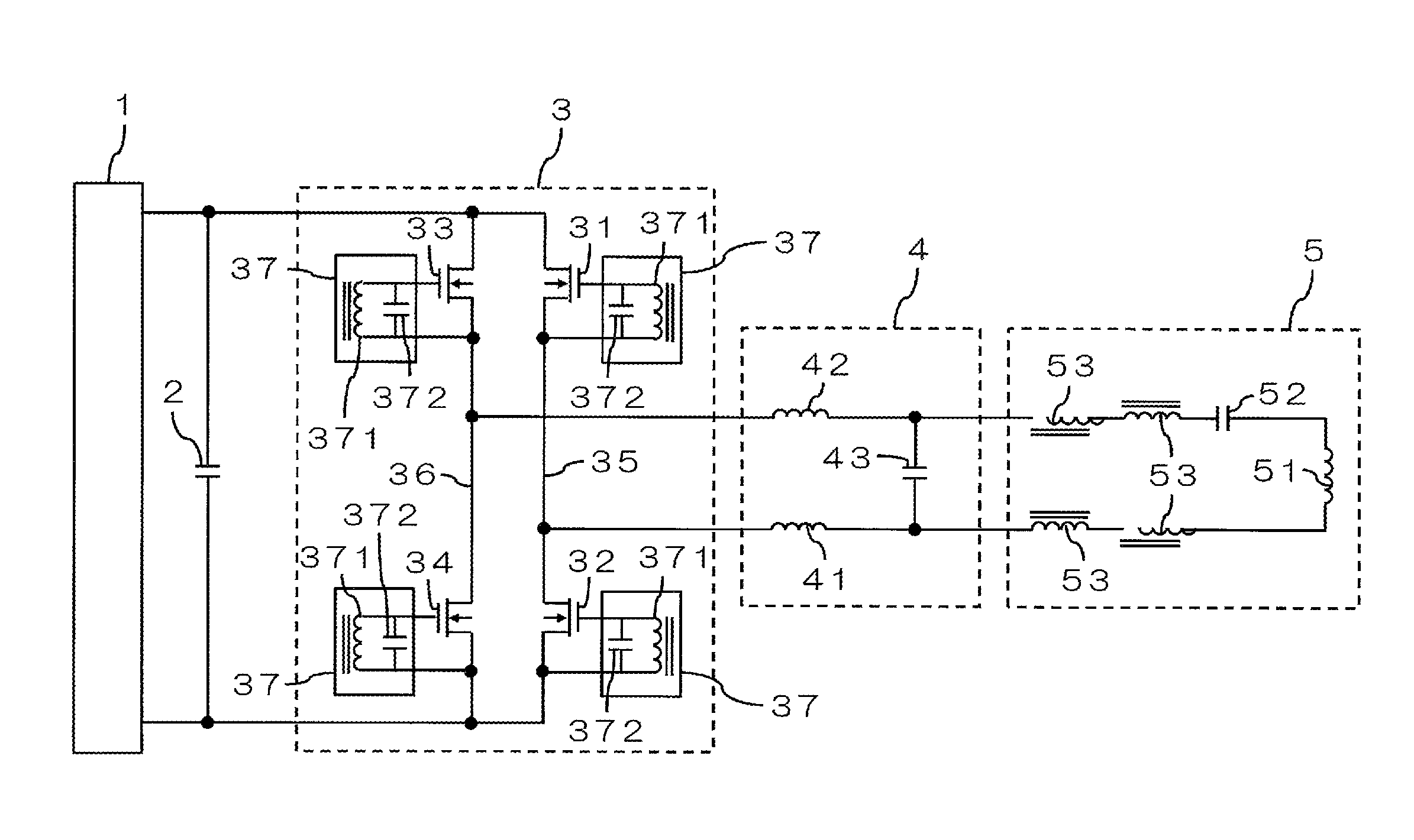
[0034]FIG. 1 is a circuit diagram showing a configuration example of a high-frequency power supply device according to an embodiment of the present invention. This high-frequency power supply device may be applied to an analysis device such as an inductively coupled plasma (ICP) emission spectrometer, and is a high-frequency power supply device of a self-oscillating method provided with a DC power supply 1, a bypass capacitor 2, a switching circuit 3, an impedance conversion circuit 4, an LC resonant circuit 5, and the like.

[0035]The DC power supply 1 sets a DC voltage of the switching circuit 3, and determines the high-frequency power to be supplied to the LC resonant circuit 5. The bypass capacitor 2 is arranged between the DC power supply 1 and the switching circuit 3, and secures a low-impedance high-frequency current path.

[0036]The LC resonant circuit 5 includes an induction coil 51, and a capacitor 52 that is connected to the induction coil 51. In this example, a series resona...


PUM


Abstract

A transformer is formed into a substantially U shape. The length of the transformer may thus be secured, and also the length of pattern wiring between an input terminal and an output terminal of a secondary coil of the transformer and the control terminals of a semiconductor device may be reduced. Moreover, the primary coil and the secondary coil of the transformer are arranged in parallel. The coupling coefficient between the primary coil and the secondary coil is thereby increased. An LC resonant circuit, not including the induction coil, and a switching circuit and the transformer are accommodated inside a housing. A water-cooling radiator is provided inside the housing, and also air inside the housing is circulated by a cooling fan while being guided to the radiator.

Description

BACKGROUND OF THE INVENTION[0001]Field of the Invention[0002]The present invention relates to a high-frequency power supply device for generating plasma by supplying high-frequency power to an induction coil included in a resonant circuit from a DC power supply via a switching circuit.[0003]Description of the Related Art[0004]For example, an analysis device such as an inductively coupled plasma (ICP) emission spectrometer has a configuration of generating plasma at a plasma torch by supplying high-frequency power to an induction coil included in a resonant circuit (for example, see JP-A-10-214698, JP-W-2009-537829, and JP-A-6-20793). A high-frequency electromagnetic field is generated by the high-frequency power supplied to the induction coil, and an induced current flows by charged particles in plasma being accelerated, and plasma is thereby heated.[0005]In the case of such a configuration, the impedance (resistance component and reactance component) of the induction coil is change...

Claims


Application Information

Patent Timeline
Patent Type & Authority Patents(United States)
IPC IPC(8): H05H1/46H01J37/32G01J3/02H05H1/36
CPCH05H1/46G01J3/027H01J37/321H01J37/32174H05H1/36H05H2001/4652H05H2001/4682H05H1/4652H05H2242/20
Inventor HABU, TOSHIYA
Owner SHIMADZU CORP
Why Eureka
Try Eureka