
Method and device for using substrate geometry to determine optimum substrate analysis sampling

a technology of substrate geometry and sampling method, applied in the field of substrate processing, can solve the problems of limited time available to make these measurements, limited number of measurements that can be made during such time, and the most significant performance problem of pattern overlay

Active Publication Date: 2017-03-07
KLA CORP
View PDF61 Cites 1 Cited by
  • Summary
  • Abstract
  • Description
  • Claims
  • Application Information

AI Technical Summary

Benefits of technology

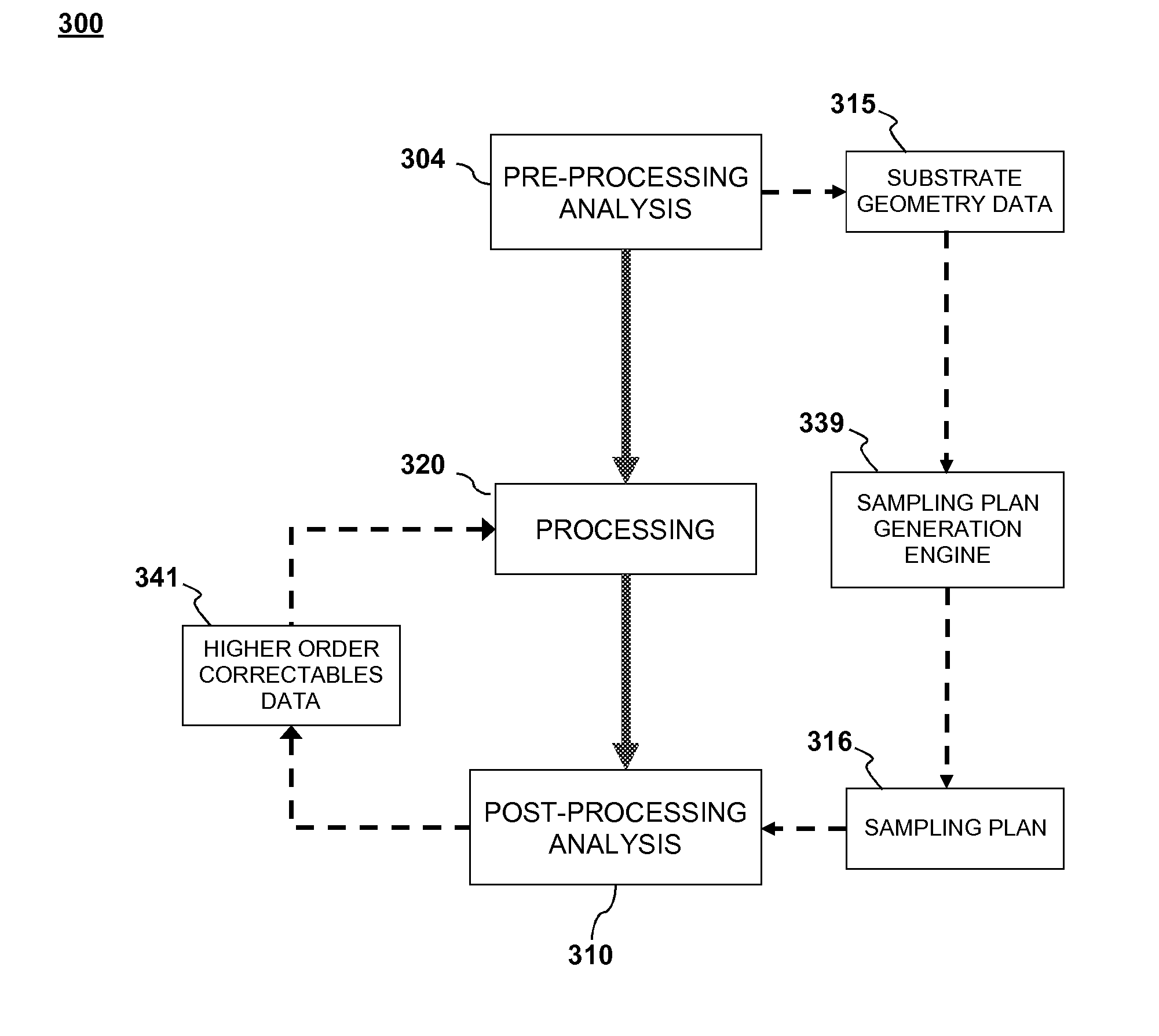
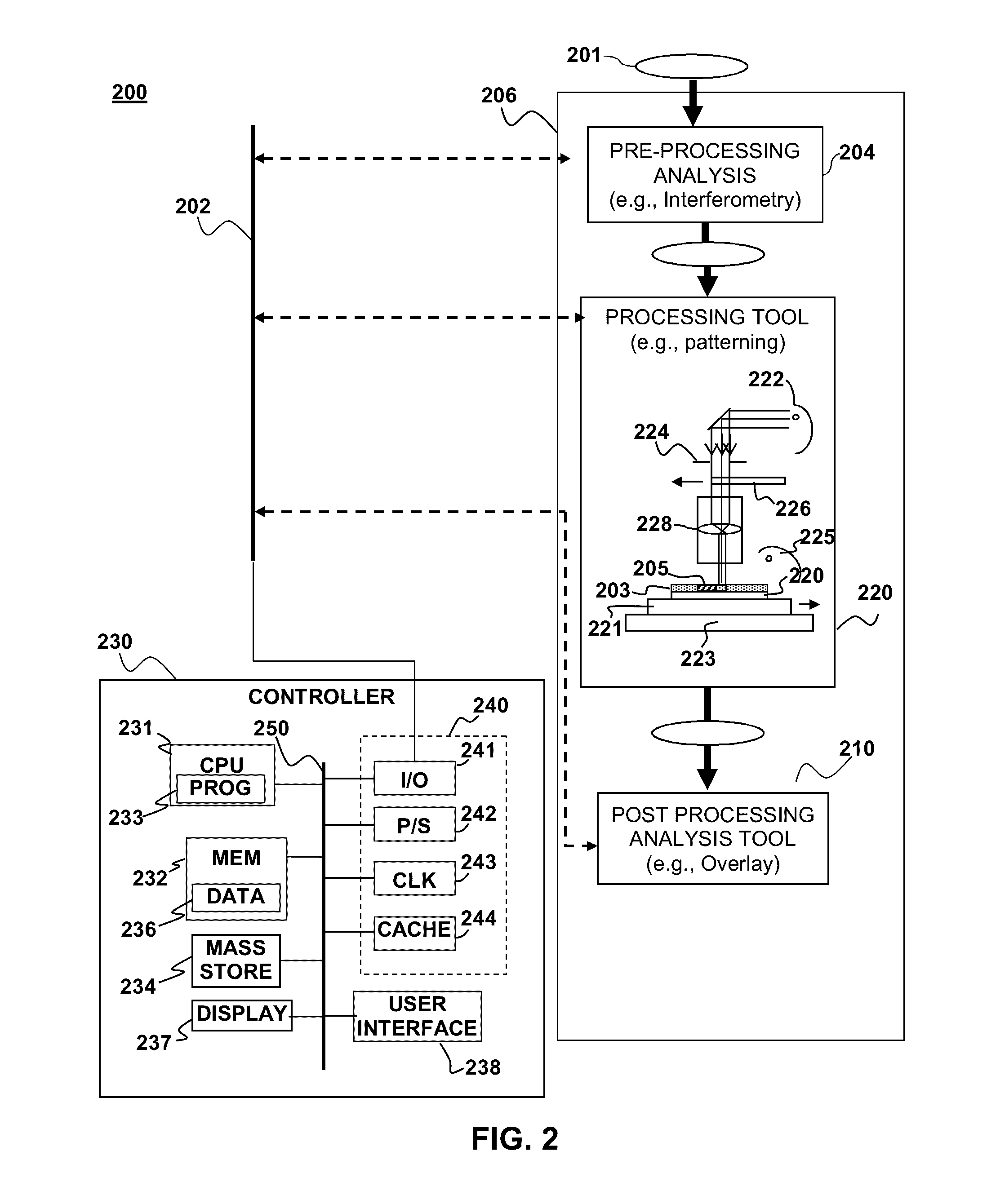
The present invention is about improving the yield of semiconductor devices by using information about the substrate geometry to generate a sampling plan for post-processing analysis. This sampling plan helps to identify areas of the substrate that have large changes in geometry and need more frequent sampling to detect and correct any residual errors. By adjusting the sampling pattern based on the substrate geometry, the method allows for better yield and reduced overlay errors. The invention also includes a process control loop that uses the substrate geometry data to generate an alignment plan for the processing tool, which helps to improve the accuracy of the alignment and reduce the number of adjustments required during the fabrication process.

Problems solved by technology

As circuit densities increase and device sizes decrease, pattern overlay is becoming one of the most significant performance issues during development of semiconductor process technology.
The time available to make these measurements is limited because these measurements have to be done while the previous wafer is being exposed (or otherwise processed).
Consequently, the number of measurements that can be made during such time is limited.
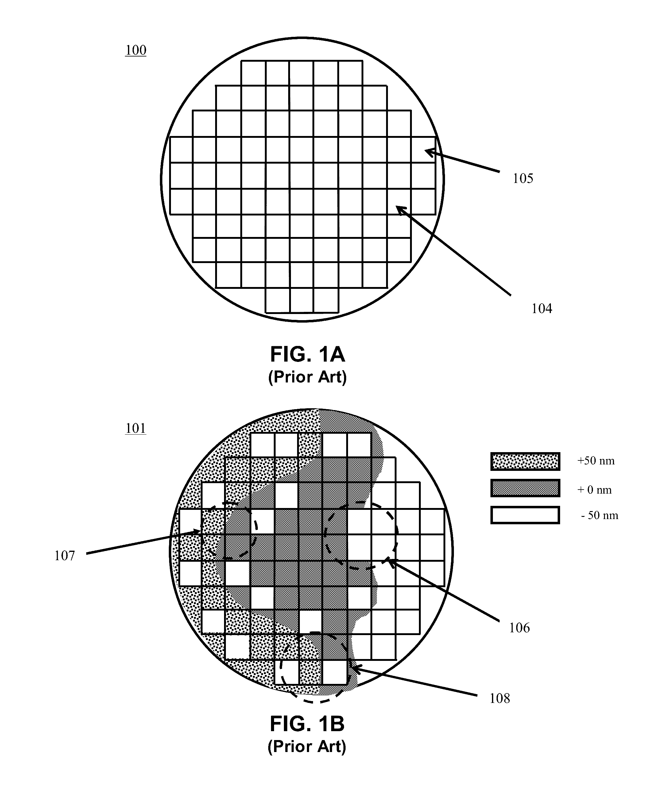
Scanners do adjust the leveling and alignment of each individual die before printing, but the leveling only corrects for average slopes in the X and Y directions (e.g., a tilted wafer plane) and not for vertical distortions on scale lengths shorter than a die.
Complex distortions of the shape of the wafer in X, Y, and Z due to the non-uniform changes in geometry from previous processing steps are not adequately accounted for by the patterning tool.
This tends to create regions of the wafer where yield is low due to poor alignment of one pattern with earlier patterns on chips in that area of the wafer.
Testing every die on a wafer is time consuming.
As a result not all dies can be tested and a sampling plan must be created.
However, it is understood in the art that overlay residual errors are often caused by changes in the wafer geometry.
When matched up against the static sampling plan it is evident that there will be several areas where overlay residual errors are likely to occur, but will not be detected by the static sampling plan.
The areas of greater change in geometry are likely sources of overlay residual errors, but they are not guaranteed to be checked.
These overlay problems may produce the need for significant amounts of rework, or even scrap.

Method used


Image

  • Method and device for using substrate geometry to determine optimum substrate analysis sampling
  • Method and device for using substrate geometry to determine optimum substrate analysis sampling
  • Method and device for using substrate geometry to determine optimum substrate analysis sampling

Examples


Embodiment Construction

[0019]Although the following detailed description contains many specific details for the purposes of illustration, anyone of ordinary skill in the art will appreciate that many variations and alterations to the following details are within the scope of the invention. Accordingly, the exemplary embodiments of the invention described below are set forth without any loss of generality to, and without imposing limitations upon, the claimed invention.

[0020]In the following description, reference is made to the accompanying drawings, which form a part hereof, and in which is shown by way of illustration specific embodiments in which embodiments of the invention may be practiced. In this regard, directional terminology, such as “top,”“bottom,”“front,”“back,”“leading,”“trailing,” etc., is sometimes used with reference to the orientation of the figure(s) being described. Because components of embodiments of the present invention can be positioned in a number of different orientations, the di...


PUM

PropertyMeasurementUnit
spatial wavelength rangeaaaaaaaaaa
heightaaaaaaaaaa
lengthaaaaaaaaaa

Abstract

A method and apparatus for process control in the processing of a substrate is disclosed in the present invention. Embodiments of the present invention utilize a first analysis tool to determine changes in a substrate's geometry. The substrate geometry data is used to generate sampling plan that will be used to check areas of the substrate that are likely to have errors after processing. The sampling plan is fed forwards to a second analysis tool that samples the substrate after it has been processed. It is emphasized that this abstract is provided to comply with the rules requiring an abstract that will allow a searcher or other reader to quickly ascertain the subject matter of the technical disclosure. It is submitted with the understanding that it will not be used to interpret or limit the scope or meaning of the claims.

Description

FIELD OF THE INVENTION[0001]Embodiments of this invention generally relate to substrate processing and more particularly to process control in substrate processing.BACKGROUND OF THE INVENTION[0002]Tighter layer to layer device overlay tolerances are needed in substrate processing (e.g., semiconductor device wafer processing) in order to meet device performance requirements and maximize the device yield. As circuit densities increase and device sizes decrease, pattern overlay is becoming one of the most significant performance issues during development of semiconductor process technology.[0003]The manufacture of modern integrated circuit chips requires many different patterns to be layered one on another. Each new pattern has to be accurately registered with patterns already on the chip. The patterning tool (e.g., a scanner or stepper) that prints the pattern on the wafer contains subsystems that measure the location, height and tilt of the existing pattern. The time available to mak...

Claims


Application Information

Patent Timeline
Patent Type & Authority Patents(United States)
IPC IPC(8): G05B11/01G03F7/20G05B19/418H01L21/67
CPCG03F7/70616G03F7/70525G03F7/70633G05B19/41875H01L21/67288Y02P90/02
Inventor MACNAUGHTON, CRAIG W.SINHA, JAYDEEP K.
Owner KLA CORP
Learn More