Semiconductor device

a technology of semiconductors and semiconductors, applied in the direction of semiconductor devices, basic electric elements, electrical equipment, etc., can solve the problems of reducing breakdown voltage, oxide film breakage, and loss of features obtained by employing a wide band gap semiconductor, so as to prevent breakdown voltage from lowering, reduce the effective resistance of the first semiconductor region, and reduce the effect of on-state resistan

Inactive Publication Date: 2017-03-14
FUJI ELECTRIC CO LTD
View PDF24 Cites 3 Cited by
  • Summary
  • Abstract
  • Description
  • Claims
  • Application Information

AI Technical Summary

Benefits of technology

[0029]According to the above aspect of the invention, the fourth semiconductor region is disposed at the semiconductor substrate side of the inner part of the second semiconductor region so as to adjoin the first semiconductor region. And then in the off-state, the spread depletion layer from the pn junction between the second semiconductor region and the fourth semiconductor region to the first semiconductor region side allows the fourth semiconductor region to be pinched off. Then this can prevent the breakdown voltage from lowering. Further, according to the invention described above, the fourth semiconductor region is disposed at the semiconductor substrate side of the inner part of the second semiconductor region so as to adjoin the first semiconductor region. And then a current that flows from the second electrode to the first electrode flows from the whole of the first semiconductor region to the fourth semiconductor region, passing through the fourth semiconductor region to flow into a JFET region (a part adjoining the gate dielectric film in the first semiconductor region). Thus the ineffective region that almost no current flows will not be formed. Therefore, it is possible to reduce effective resistance of the first semiconductor region.
[0030]According to the semiconductor device of the present invention, there is provided a beneficial effect that on-state resistance thereof can be reduced without the degradation of breakdown voltage.

Problems solved by technology

Then this causes features obtained by employing the wide band gap semiconductor to be lost.
And then this causes adverse effects such as oxide film breakage and the breakdown voltage lowering.
Along with this, there is a new problem that the on-state voltage increases owing to cell density decline.

Method used


Image

  • Semiconductor device
  • Semiconductor device
  • Semiconductor device

Examples


first embodiment

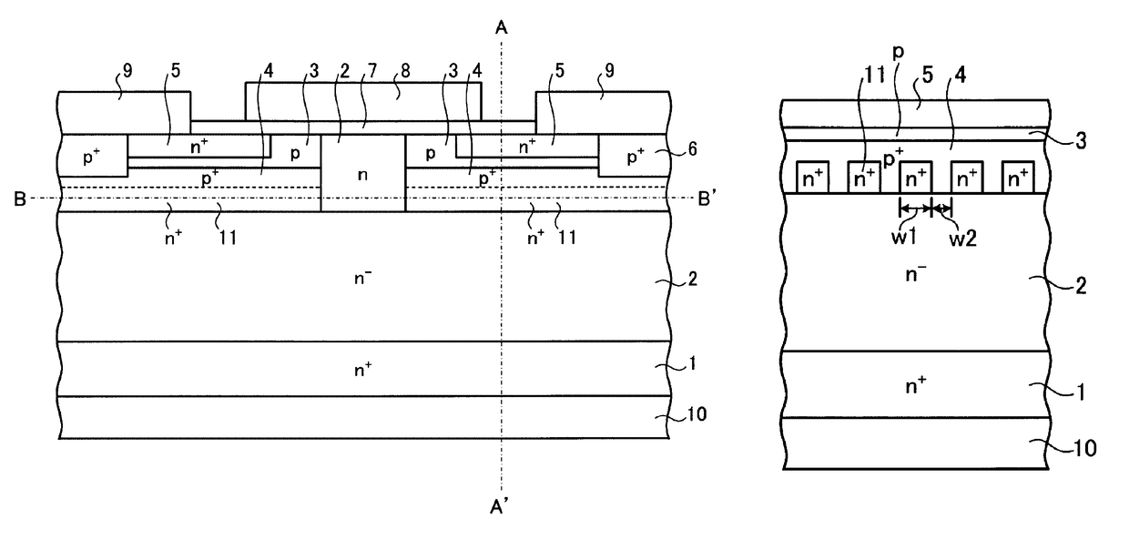
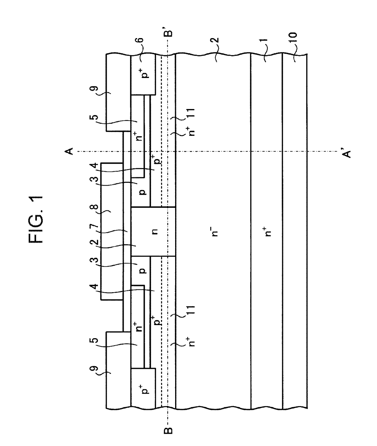
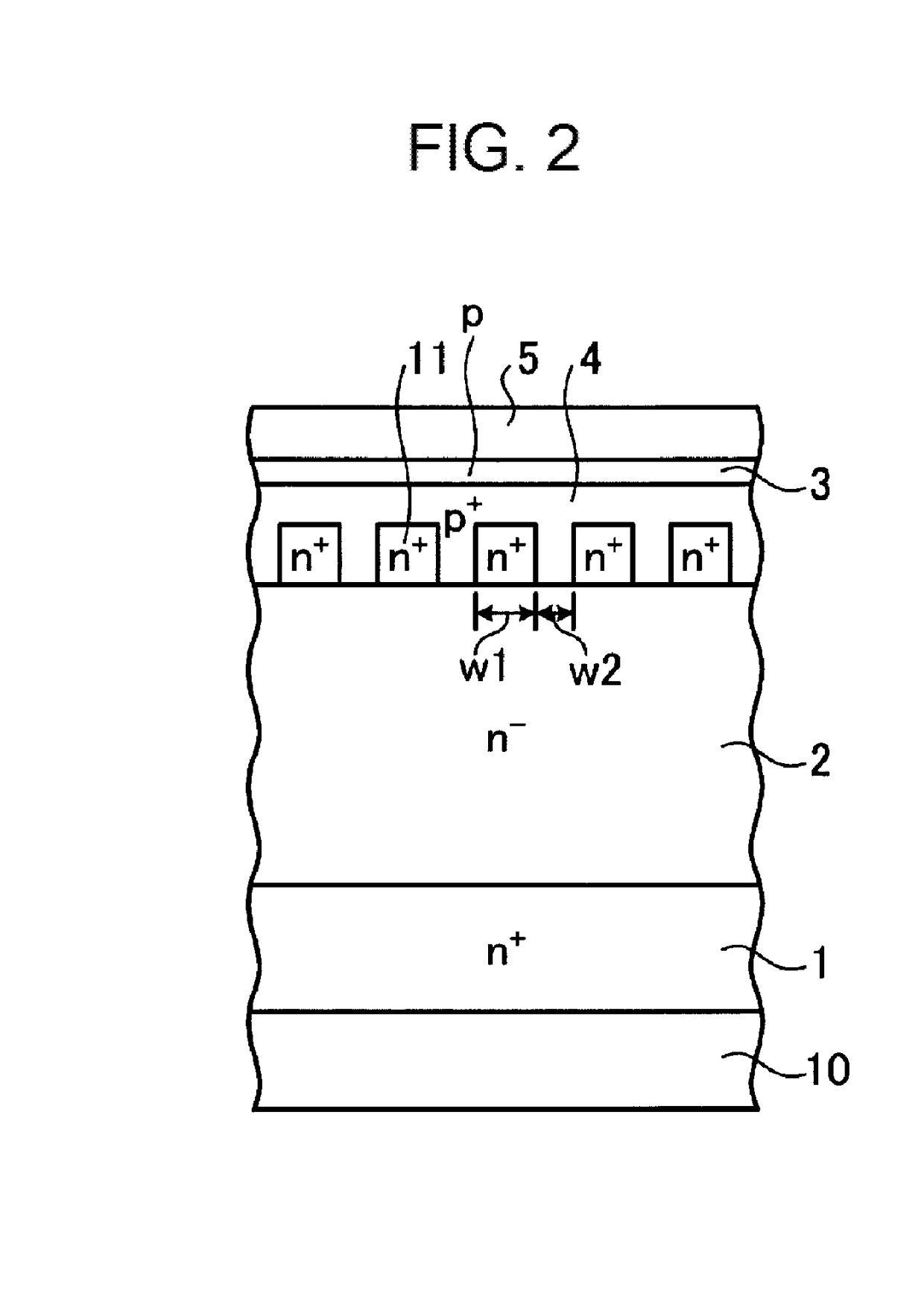
[0046]A structure of a semiconductor device according to the first embodiment will be described. FIG. 1 is a sectional view illustrating a structure of a semiconductor device according to the first embodiment. FIG. 2 is a sectional view cut along the line A-A′ shown in FIG. 1. FIG. 3 is a plan view cut along the line B-B′ shown in FIG. 1. The semiconductor device according to the first embodiment shown in FIG. 1 is a wide band gap semiconductor device fabricated using a semiconductor material having a band gap wider than silicon (Si) such as silicon carbide (SiC), gallium nitride (GaN), or diamond (wide band gap semiconductor). FIG. 1 shows a cell structure of the wide band gap semiconductor device. FIG. 3 shows a situation that the cell structure shown in FIG. 1 is arranged in parallel.

[0047]In the wide band gap semiconductor device shown in FIGS. 1 to 3, an n− drift region (a first semiconductor region) 2 is disposed by epitaxial growth on the front surface of an n+ semiconductor ...

second embodiment

[0057]Next, a structure of a semiconductor device according to the second embodiment will be described. FIG. 5 is a plan view illustrating the structure of the semiconductor device according to the second embodiment. The semiconductor device according to the second embodiment is different from that according to the first embodiment in that there is disposed a high-concentration base region 24 having a hexagonal planar figure. In this case, a contact region (not shown) has the polygonal (for example hexagonal) planar figure, and the high-concentration base region 24 is disposed so as to surround the circumference of the end portion of the contact region located at the semiconductor substrate 1 side. An high-concentration region 21 is, for example, arranged by a stripe-shaped planar layout extending from the hexagonal center of the high-concentration base region 24 to each of the sides. A reference numeral 22a corresponds to the JFET region. A reference numeral 29a corresponds to the ...

third embodiment

[0059]Next, a structure of a semiconductor device according to the third embodiment will be described. FIG. 6 is a sectional view illustrating the structure of the semiconductor device according to the third embodiment. The semiconductor device according to the third embodiment is different from that according to the first embodiment in that the impurity concentration of an n+ high-concentration region 31 is set to be lower at the semiconductor substrate 1 side thereof than that at the p-channel region 3 side thereof. Concretely, the high-concentration region 31 is composed of a first high-concentration region 31a located at the p-channel region 3 side thereof and a second n high-concentration region 31b, whose concentration is lower than that of the first n+ high-concentration region 31a, located at the n+ semiconductor substrate 1 side thereof.

[0060]An impurity concentration distribution of the n+ high-concentration region 31 in the semiconductor device according to the third embo...


PUM


Abstract

An n− drift region is disposed on the front surface of an n+ semiconductor substrate composed of a wide band gap semiconductor. A p-channel region is selectively disposed on the surface layer of the n− drift region. A high-concentration p+ base region is disposed so as to adjoin the lower portion of the p-channel region inside the n− drift region. Inside the high-concentration p+ base region, an n+ high-concentration region is selectively disposed at the n+ semiconductor substrate side. The n+ high-concentration region has a stripe-shaped planar layout extending to the direction that the high-concentration p+ base regions line up. The n+ high-concentration region adjoins a JFET region at one end portion in longitudinal direction of the stripe. Further, the n+ semiconductor substrate side of the n+ high-concentration region adjoins the part sandwiched between the high-concentration p+ base region and the n+ semiconductor substrate in the n− drift region.

Description

[0001]This application is a continuation under 35 U.S.C. 120 of International Application PCT / JP2013 / 053439 having the International Filing Date of Feb. 13, 2013. The identified application is fully incorporated herein by reference.BACKGROUND[0002]Technical Field[0003]This invention relates to a semiconductor device.[0004]Background Art[0005]It is expected that semiconductor materials such as silicon carbide (SiC), gallium nitride (GaN), and diamond, which have band gaps wider than silicon (hereinafter, described as wide band gap semiconductors), are applied to power devices especially because of excellent characteristics such as a high dielectric breakdown field and high thermal conductivity. For conventional power devices, for example, a vertical MOSFET (metal oxide field effect transistor) fabricated by using SiC (hereinafter, SiC vertical MOSFET), will be described. FIG. 14 is a sectional view illustrating a structure of the conventional SiC vertical MOSFET.[0006]As shown in FIG...

Claims


Application Information

Patent Timeline
Patent Type & Authority Patents(United States)
IPC IPC(8): H01L29/78H01L21/04H01L29/06H01L29/66H01L29/739H01L29/08H01L29/10H01L29/20H01L29/16
CPCH01L29/7802H01L21/046H01L29/0634H01L29/0684H01L29/0878H01L29/0886H01L29/1095H01L29/66068H01L29/7395H01L29/1602H01L29/1608H01L29/2003
Inventor KUMAGAI, NAOKI
Owner FUJI ELECTRIC CO LTD
Why Eureka
Try Eureka