Solar cell
a solar cell and cell technology, applied in the field of solar cells, can solve the problems of low current conversion efficiency of solar cells, and achieve the effects of excellent chemical passivation characteristic, excellent field effect passivation characteristic, and excellent abrasion resistan
- Summary
- Abstract
- Description
- Claims
- Application Information
AI Technical Summary
Benefits of technology
Problems solved by technology
Method used
Image
Examples
first embodiment
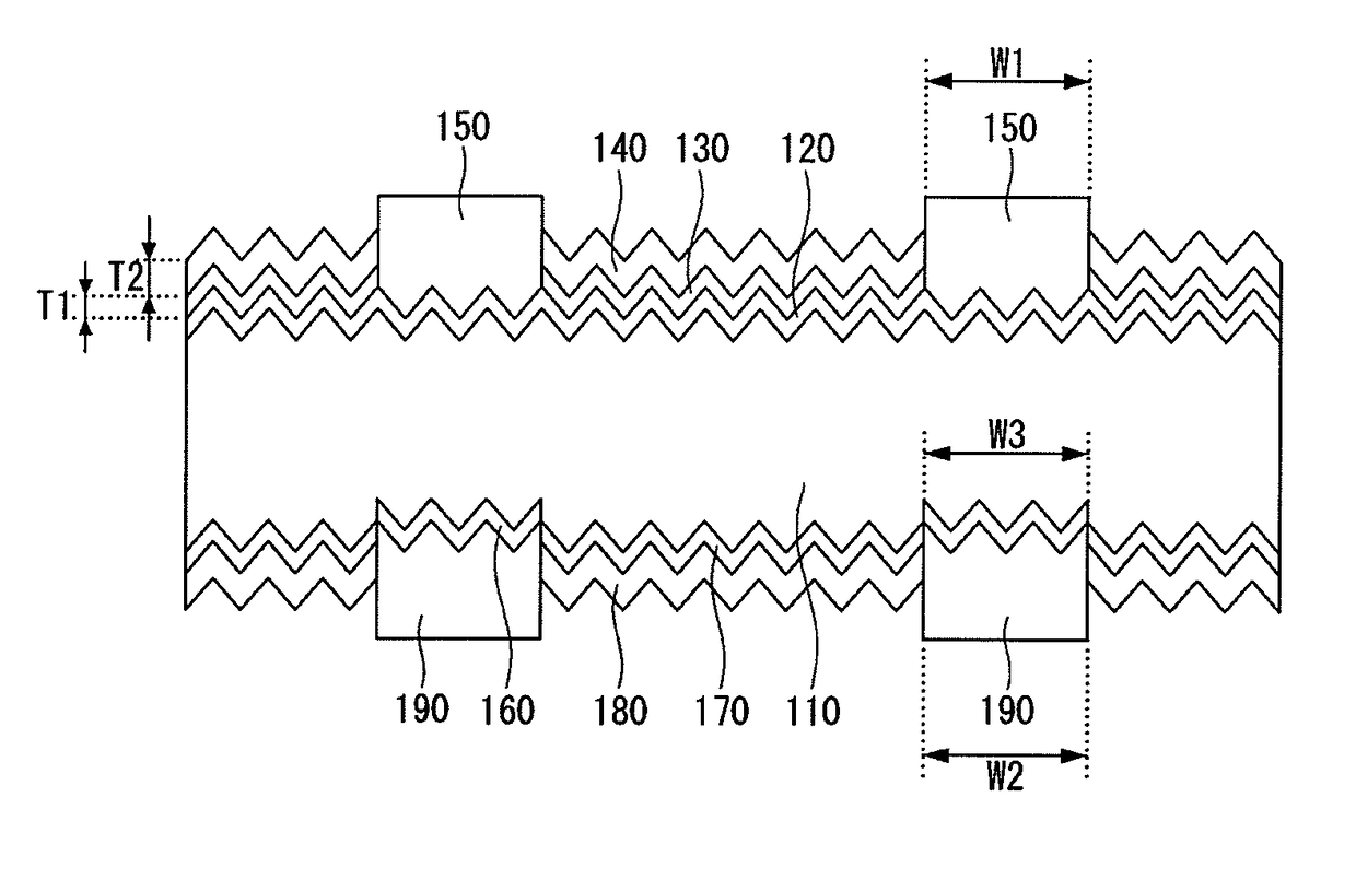
[0033]FIG. 1 is a schematic cross-sectional view of a solar cell according to the invention.
[0034]As shown in FIG. 1, a solar cell according to a first embodiment of the invention includes a substrate 110, an emitter layer 120 positioned at one surface of the substrate 110, for example, a front surface of the substrate 110, a first protective layer 130 positioned on the emitter layer 120, a first anti-reflection layer 140 positioned on the first protective layer 130, a plurality of first electrodes 150 positioned on the emitter layer 120 where the first protective layer 130 and the first anti-reflection layer 140 are not positioned, a back surface field (BSF) layer 160 positioned at a back surface of the substrate 110, a second protective layer 170 positioned on the back surface of the substrate 110, a second anti-reflection layer 180 positioned on a back surface of the second protective layer 170, and a plurality of second electrodes 190 positioned on a back surface of the back sur...
second embodiment
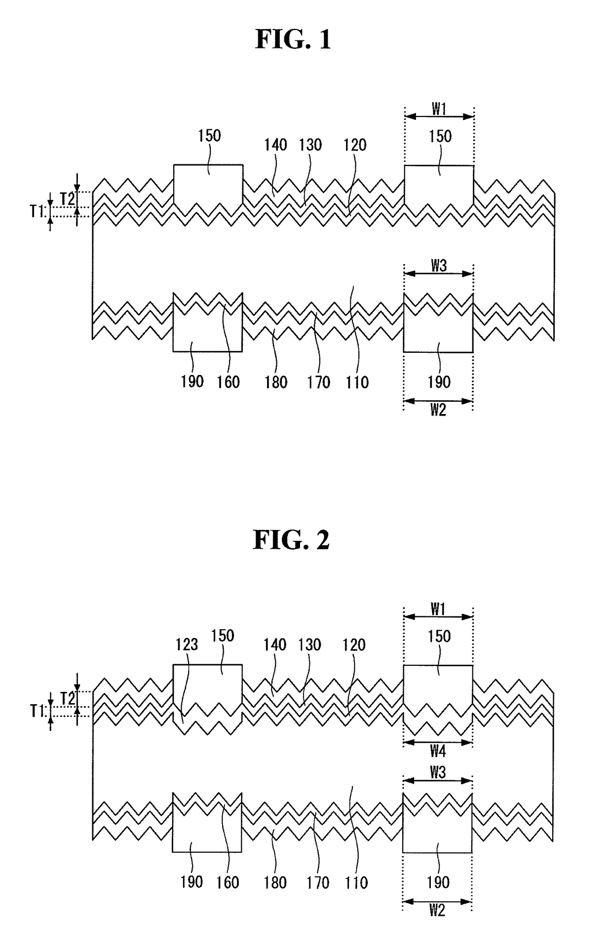
[0061]A solar cell according to the invention is described below with reference to FIG. 2.
[0062]Since the solar cell according to the second embodiment of the invention is substantially the same as the solar cell according to the first embodiment of the invention except an emitter layer, a further description may be briefly made or may be entirely omitted. Hereinafter, only a configuration of the emitter layer is described.
[0063]The emitter layer 120 according to the first embodiment of the invention has a uniform doping concentration throughout the entire area of the emitter layer 120. Thus, the emitter layer 120 according to the first embodiment of the invention may be easily manufactured through a simple process, but a recombination of carriers of the emitter layer 120 may increase because of a high doping concentration. As a result, an improvement in the efficiency of the solar cell may be limited.
[0064]Accordingly, the emitter layer 120 according to the second embodiment of the...
PUM
 Abstract
Description
Claims
Application Information


