Method for determining the phase angle and/or the thickness of a contamination layer at an optical element and EUV lithography apparatus

a technology of euv lithography and optical elements, which is applied in the direction of optical radiation measurement, printers, instruments, etc., can solve the problems of forming a contamination layer at the optical elements, and achieve the effect of simplifying the implementation of this method

Active Publication Date: 2017-04-11
CARL ZEISS SMT GMBH
View PDF15 Cites 0 Cited by
  • Summary
  • Abstract
  • Description
  • Claims
  • Application Information

AI Technical Summary

Benefits of technology

[0009]It is an object of the invention to develop a method of the type mentioned in the introduction such that it can be used during the operation of an EUV lithography apparatus. A further object is to provide an EUV lithography apparatus which simplifies the implementation of this method.
[0021]In one advantageous variant, a charge amplifier is used for measuring the photocurrent generated during the irradiation. A charge amplifier is a charge-voltage converter which converts the input charge arriving at a signal input into a voltage value proportional to the input charge at the signal output. The proportionality constant between input charge and output voltage determines the gain of the charge amplifier. The inventor has recognized that, in the case of the present use in EUV lithography apparatuses, only very few charges or electrons are generated as a result of the photoelectric effect. The charge amplifier makes it possible to significantly increase the measurement accuracy when determining the phase angle and / or the thickness of the contamination layer in comparison with the use e.g. of an ammeter (without a charge amplifier). Moreover, the output signal of the charge amplifier, particularly if the latter has a low output impedance, can be transmitted in a manner free of interference and without problems even over relatively large distances.
[0023]In one embodiment, the charge amplifier is arranged at a distance of less than 150 cm, preferably of less than 50 cm, from the optical element. In particular, the charge amplifier can be arranged in the region of a mount or holder for the optical element. The arrangement of the charge amplifier in proximity to the optical element has proved to be advantageous for avoiding conduction losses and minimizing electromagnetic noise. The charge amplifier can be arranged within the vacuum environment in which the optical element is also situated, but it is also possible to arrange the charge amplifier outside the vacuum environment and to lead the line or the cable out of the vacuum environment. In this way, the exchange or maintenance of the charge amplifier is simplified, but this advantage is bought at the expense of a considerable increase in the electromagnetic noise.
[0028]In a further embodiment, the EUV lithography apparatus comprises a calibration light source for irradiating the optical element with calibration radiation at wavelengths that are not reflected by the multilayer coating. The calibration radiation can be for example radiation which is generated by a calibration light source in a wavelength range of between 9 nm and 11 nm or between 14 nm and 16 nm. Alternatively or additionally, it is also possible to use radiation in the UV range or in the visible wavelength range, for example at wavelengths of between approximately 190 nm and 450 nm, which can be generated for example by laser diodes or by a broadband light source. The use of calibration radiation in the UV range or in the visible range is advantageous since this radiation can be fed to the optical element via an optical fiber. Feeding with free beam propagation is also possible.

Problems solved by technology

Since optical elements that reflect EUV radiation are typically operated in a vacuum environment in a residual gas atmosphere in which the occurrence of contaminating gaseous substances cannot completely be avoided, a contamination layer often forms at the optical elements.
However, the photocurrent should be measured at a point in time at which there is no or only a very small content of activated hydrogen in the residual gas atmosphere surrounding the optical element, since said activated hydrogen forms free radicals (H+) which can corrupt the measurement result.

Method used


Image

  • Method for determining the phase angle and/or the thickness of a contamination layer at an optical element and EUV lithography apparatus
  • Method for determining the phase angle and/or the thickness of a contamination layer at an optical element and EUV lithography apparatus
  • Method for determining the phase angle and/or the thickness of a contamination layer at an optical element and EUV lithography apparatus

Examples


Embodiment Construction

[0036]In the following description of the drawings, identical reference signs are used for identical or functionally identical components.

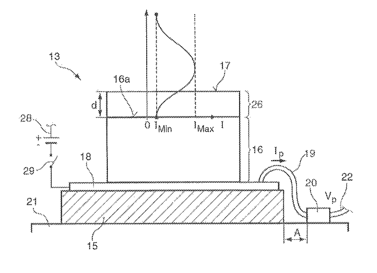
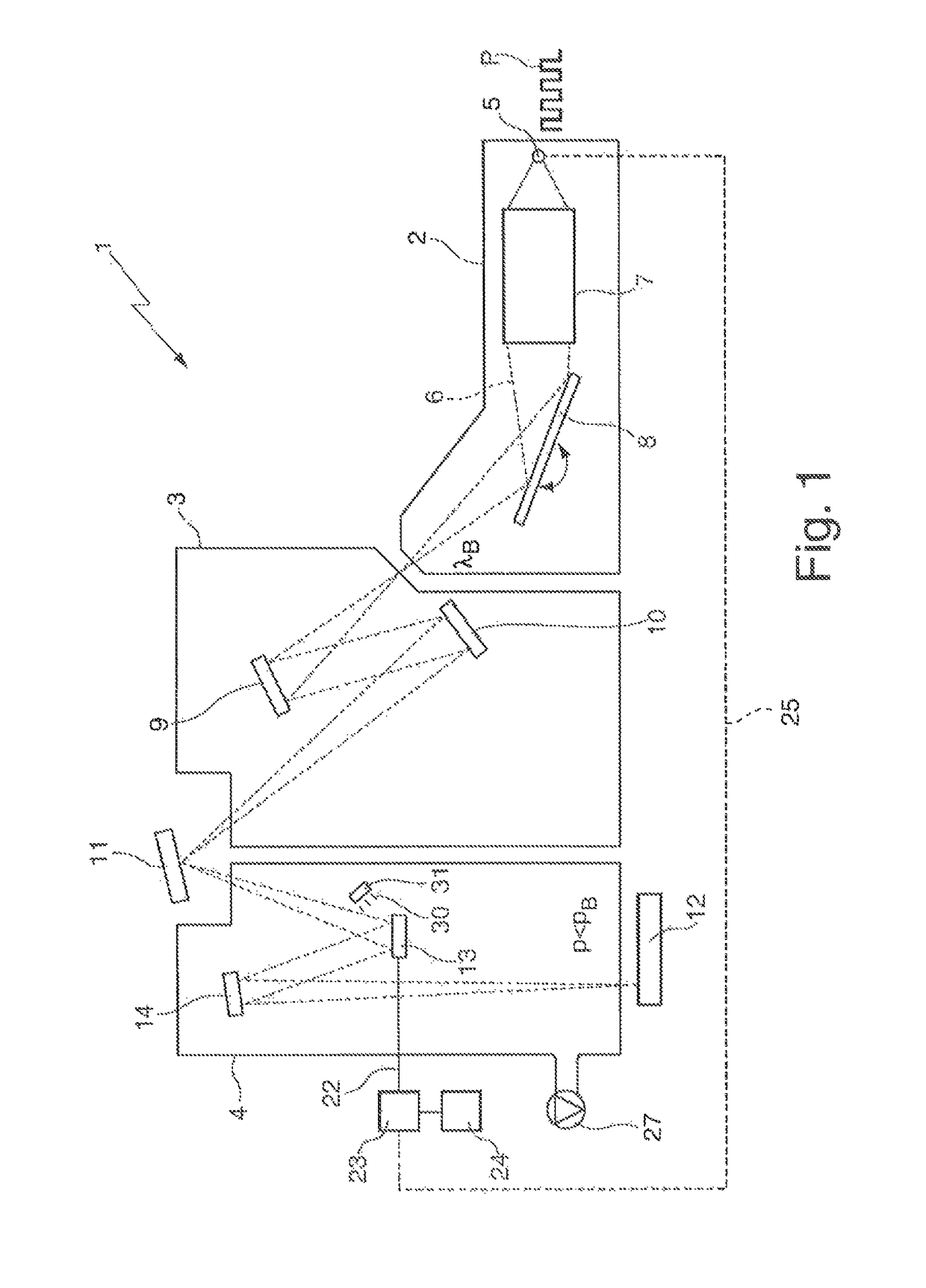
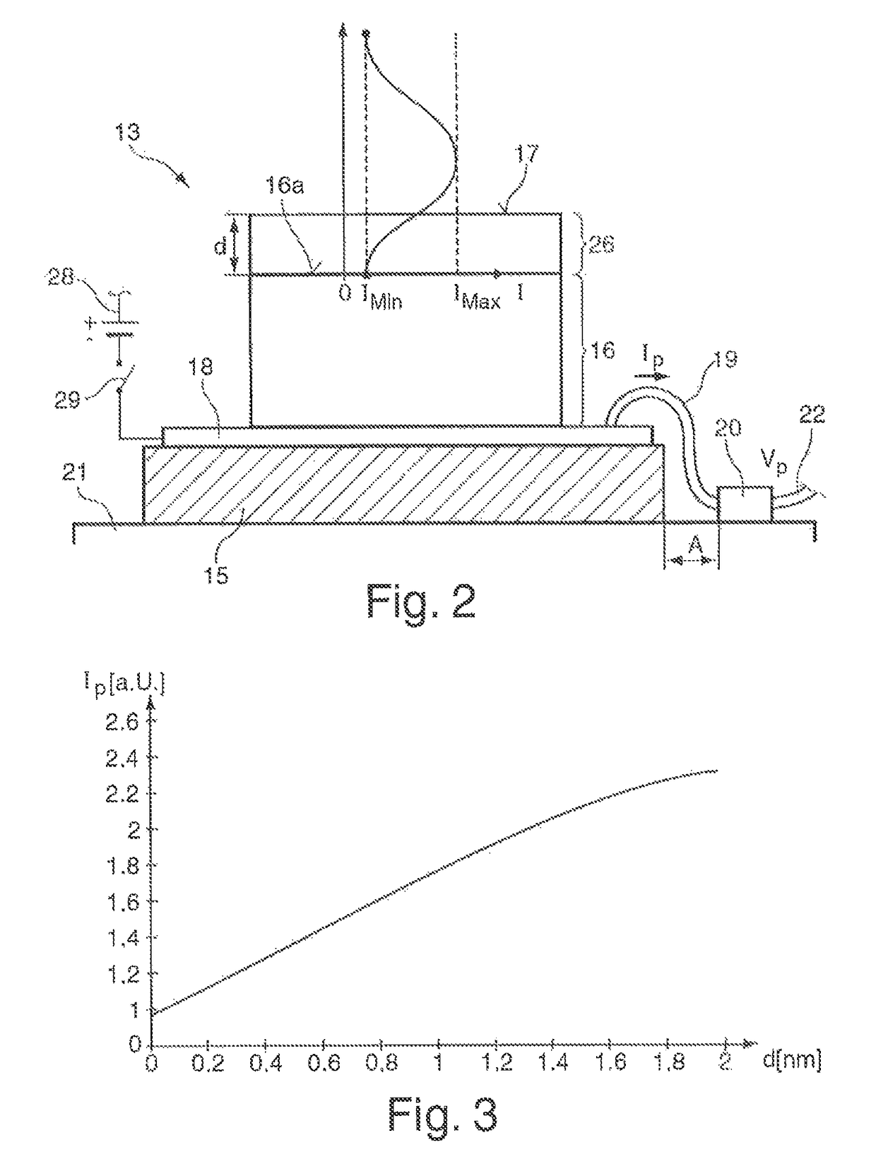
[0037]FIG. 1 schematically shows an EUV lithography apparatus in the form of a projection exposure apparatus 1 for EUV lithography. The projection exposure apparatus 1 has a beam generating system2, an illumination system 3 and a projection system 4, which are accommodated in separate vacuum housings and arranged successively in a beam path 6 proceeding from an EUV light source 5 of the beam shaping system 2. By way of example, a plasma source or a synchrotron can serve as the EUV light source 5. The radiation in the wavelength range of between approximately 5 nm and approximately 20 nm emerging from the light source 5 is firstly focused in a collimator 7. With the aid of a downstream monochromator 8, the desired operating wavelength λB, which is approximately 13.5 nm in the present example, is filtered out by variation of the angle of incidence, ...


PUM

PropertyMeasurementUnit
distanceaaaaaaaaaa
ultraviolet wavelengthsaaaaaaaaaa

Abstract

A method and associated EUV lithography apparatus for determining the phase angle at a free interface (17) of an optical element (13) provided with a multilayer coating (16) that reflects EUV radiation and / or for determining the thickness (d) of a contamination layer (26) formed on the multilayer coating (16). The multilayer coating (16) is irradiated with EUV radiation, a photocurrent (IP) generated during the irradiation is measured, and the phase angle at the free interface (17) and / or the thickness (d) of the contamination layer (26) is determined on the basis of a predefined relationship between the phase angle and / or the thickness (d) and the measured photocurrent (IP). The measured photocurrent (IP) is generated from the entire wavelength and angle-of-incidence distribution of the EUV radiation impinging on the multilayer coating (16).

Description

CROSS-REFERENCE TO RELATED APPLICATIONS[0001]This application is a Continuation of International Application No. PCT / EP2013 / 074170, filed on Nov. 19, 2013, which claims benefit under 35 U.S.C. §119(e) to U.S. Provisional Application No. 61 / 756,640, filed Jan. 25, 2013, and which claims priority under 35 U.S.C. §119(a) to German Patent Application No. 10 2013 201 193.8, also filed on Jan. 25, 2013. The disclosures of all three related applications are considered part of and are incorporated by reference into the disclosure of the present application in their respective entireties.FIELD AND BACKGROUND OF THE INVENTION[0002]The invention relates to a method for determining the phase angle at a free interface of an optical element provided with a multilayer coating that reflects EUV radiation and / or for determining the thickness of a contamination layer formed on the multilayer coating. The invention also relates to an EUV lithography apparatus, comprising: at least one optical element ...

Claims


Application Information

Patent Timeline
Patent Type & Authority Patents(United States)
IPC IPC(8): G03B27/54B82Y10/00G01N21/84G01N21/41G21K1/06G03F7/20G01N21/94G01B11/06G01J1/02G01J1/42
CPCG01J1/0238B82Y10/00G01B11/06G01B11/0616G01J1/429G01N21/41G01N21/8422G01N21/94G03F7/20G03F7/7085G03F7/70141G03F7/70591G03F7/70858G03F7/70908G03F7/70916G03F7/70958G21K1/062
Inventor GERHARD, MICHAEL
Owner CARL ZEISS SMT GMBH
Why Eureka
Try Eureka