
Integrated circuit device system with elevated stacked configuration and method of manufacture thereof

Active Publication Date: 2017-05-09
SMART MODULAR TECH
View PDF19 Cites 1 Cited by
  • Summary
  • Abstract
  • Description
  • Claims
  • Application Information

AI Technical Summary

Benefits of technology

This patent describes a method of manufacturing an integrated circuit device system by mounting an outer chip assembly and a mirrored chip assembly on a module interposer, which is then attached to a carrier. The carrier includes a first side and a second side, and the mirrored chip assembly is suspended above the carrier's first side. The technical effect of this invention is the improved performance and reliability of high-density integrated circuit devices.

Problems solved by technology

Attempts have failed to provide a complete solution addressing simplified manufacturing processing, smaller dimensions, lower costs due to design flexibility, increased functionality, leveragability, and increased IO connectivity capabilities.
Solutions to these problems have been long sought but prior developments have not taught or suggested any solutions and, thus, solutions to these problems have long eluded those skilled in the art.

Method used


Image

  • Integrated circuit device system with elevated stacked configuration and method of manufacture thereof
  • Integrated circuit device system with elevated stacked configuration and method of manufacture thereof
  • Integrated circuit device system with elevated stacked configuration and method of manufacture thereof

Examples


first embodiment

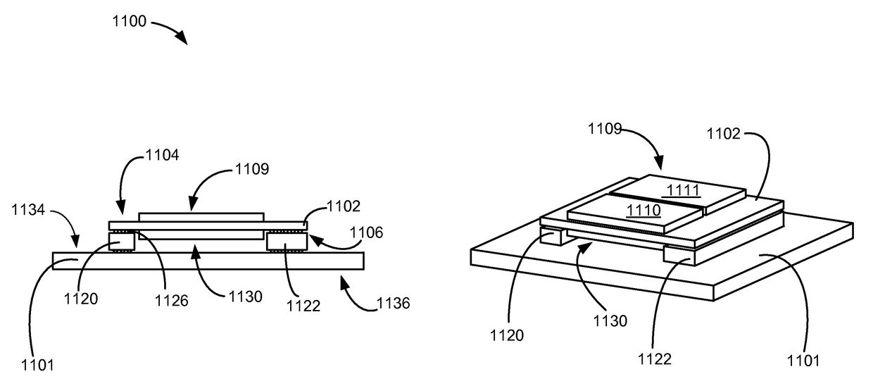
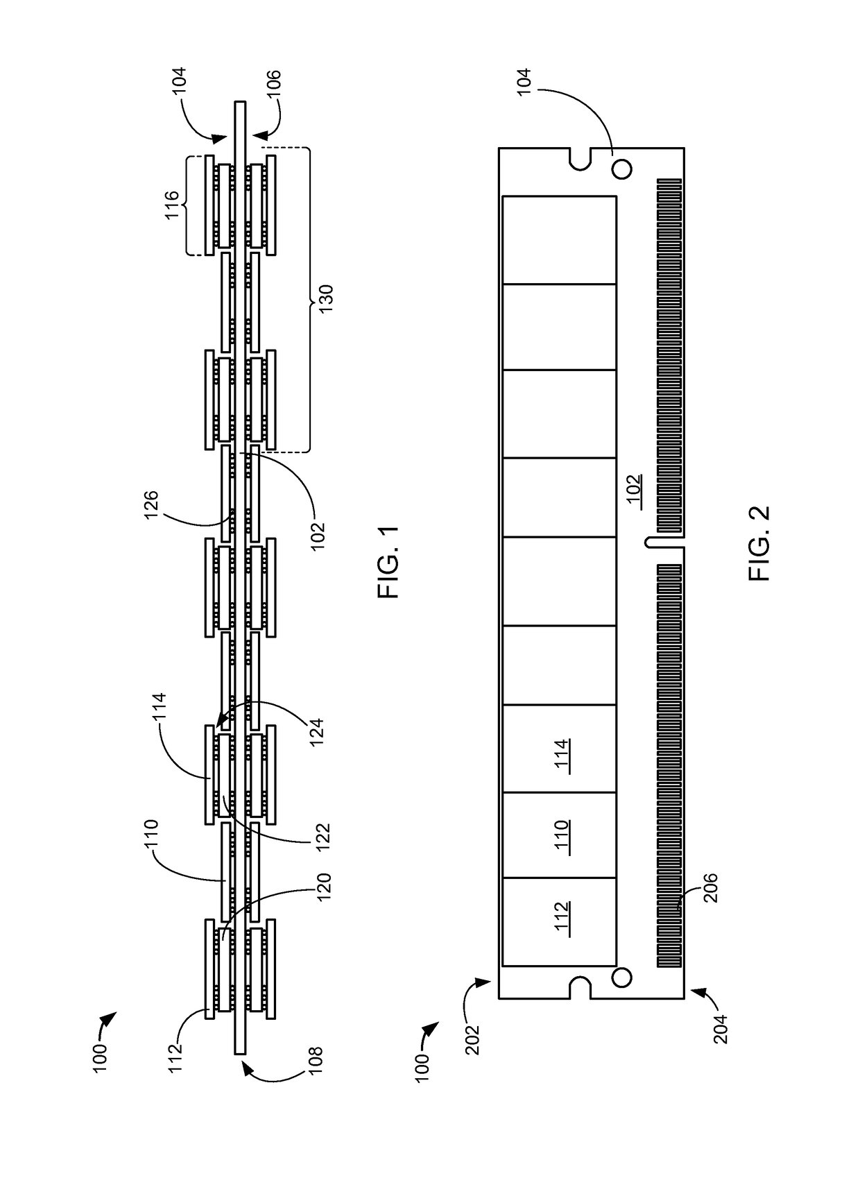
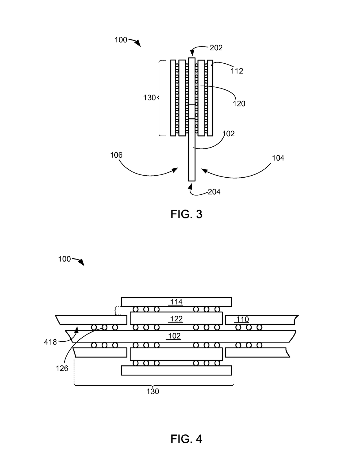
[0037]Referring now to FIG. 1, therein is shown a top view of an integrated circuit device system 100 in the present invention. The top view can depict a view of the integrated circuit device system 100 that is inserted into another system or device (both not shown). The integrated circuit device system 100 can include a carrier 102, integrated circuit devices, a first riser 120, and a second riser 122.

[0038]The carrier 102 provides structural support for components and semiconductor devices mounted thereon. For example, the carrier 102 can be a printed circuit board (PCB) for mounting memory device such as dynamic random access memory (DRAM) module units.

[0039]Further for example, the carrier can be a substrate including semi-conductive material, a core of conductive material, metal, or alloy such as copper as an example. The carrier 102 can include a first side 104 and a second side 106 opposite to the first side 104. The carrier 102 can also include a peripheral end 108, which is...

second embodiment

[0083]Referring now to FIG. 6, therein is shown a top view of an integrated circuit device system 600 in the present invention. The integrated circuit device system 600 and be identical to the integrated circuit device system 100 of FIG. 1 except that the integrated circuit device system 600 can include a first riser 602 and a second riser 604, both with a “T-shaped” configuration.

[0084]It is understood that the integrated circuit device system 600 can include identical elements and components as the integrated circuit device system 100. For example, the integrated circuit device system 600 can include the base device 110, the peripheral stacked device 112, the inner stacked device 114, and the device interconnect 126 of FIG. 1.

[0085]The first riser 602 can include a body portion 606 and a protrusion portion 608. The body portion 606 of the first riser 602 provides a base for components and devices mounted thereon. The body portion 606 is mounted directly to the carrier 102. The fir...

third embodiment

[0109]Referring now to FIG. 9, therein is shown top view of an integrated circuit device system 900 in the present invention. The integrated circuit device system 900 and be identical to the integrated circuit device system 600 of FIG. 6 except that the integrated circuit device system 900 can include a first riser 902, a second riser 904, and a third riser 906. The first riser 902, the second riser 904, and the third riser 906 can each include a “T-shaped” configuration.

[0110]It is understood that the integrated circuit device system 900 can include identical elements and components as the integrated circuit device system 100 of FIG. 1 and the integrated circuit device system 600 of FIG. 6. For example, the integrated circuit device system 900 can include the base device 110, the peripheral stacked device 112, the inner stacked device 114, and the device interconnect 126 of FIG. 6.

[0111]The second riser 904 can be identical to the second riser 604 of FIG. 6. For example, the second...


PUM


Abstract

A system and method of manufacture of an integrated circuit device system includes: a module interposer having a module first side and a module second side; an outer chip assembly mounted to the module first side; a mirrored chip assembly mounted to the module second side, the mirrored chip assembly below the outer chip assembly; and a carrier attached to the module second side, the carrier includes a carrier first side and a carrier second side, the mirrored chip assembly suspended above the carrier first side.

Description

CROSS-REFERENCE TO RELATED APPLICATION(S)[0001]This is a continuation-in-part of co-pending U.S. patent application Ser. No. 14 / 077,908 filed Nov. 12, 2013.TECHNICAL FIELD[0002]The present invention relates generally to an integrated circuit device system, and more particularly to a system with an elevated stacked configuration.BACKGROUND ART[0003]There is a continual need in the area of electronics and electronic computing systems toward smaller systems and / or systems with greater computing performance for a given space. Within these systems, the integrated circuit and memory modules are the building block used in a high performance electronic system to provide applications for usage in products such as automotive vehicles, computers, cell phone, intelligent portable military devices, aeronautical spacecraft payloads, and a vast line of other similar products that require small compact electronics supporting many complex functions.[0004]Products must compete in world markets and at...

Claims


Application Information

Patent Timeline
IPC IPC(8): H05K1/11H05K1/14H05K3/30H05K1/18
CPCH05K3/306H05K1/181H05K3/301H05K3/303H05K3/3436H05K2201/10159Y02P70/50
Inventor IYER, SATYANARAYAN SHIVKUMARPAULEY, JR., ROBERT S.MAHRAN, VICTOR
Owner SMART MODULAR TECH
Features
  • Generate Ideas
  • Intellectual Property
  • Life Sciences
  • Materials
  • Tech Scout
  • Unparalleled Data Quality
  • Higher Quality Content
  • 60% Fewer Hallucinations
Learn More