Volatile semicondcutor memory device, refresh control circuit and method thereof

a semi-conductor memory and control circuit technology, applied in the direction of information storage, static storage, digital storage, etc., can solve the problem of extremely large circuit scale, and achieve the effect of reducing consumption power and simple circuit structur

Active Publication Date: 2017-05-16
POWERCHIP SEMICON MFG CORP
View PDF14 Cites 16 Cited by
  • Summary
  • Abstract
  • Description
  • Claims
  • Application Information

AI Technical Summary

Benefits of technology

[0041]According to the refresh control circuit and the refresh control method of the volatile semiconductor memory device of the present invention, a circuit structure more simple than that of the conventional technique is adopted to control a refresh perio

Problems solved by technology

However, a refresh control circuit of the patent literature 1 has a following problem, i.e. the first current generating circuit, the second current

Method used


Image

  • Volatile semicondcutor memory device, refresh control circuit and method thereof
  • Volatile semicondcutor memory device, refresh control circuit and method thereof
  • Volatile semicondcutor memory device, refresh control circuit and method thereof

Examples


embodiment 1

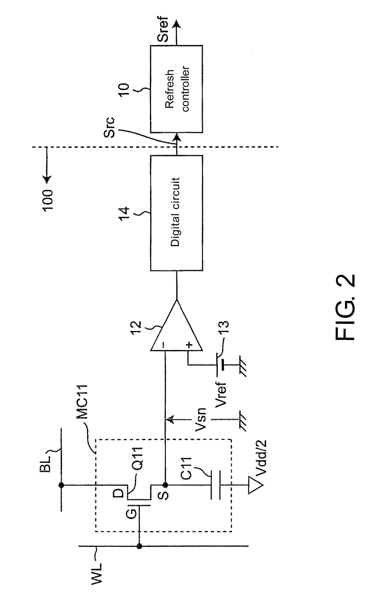
[0060]FIG. 2 is a circuit diagram of a structure example of a level-determination memory cell MC11 different to the memory cell MC1 of the DRAM and a refresh control circuit according to the embodiment 1 of the invention, FIG. 3 is a planar diagram of a layout of the DRAM using the refresh control circuit of FIG. 2. The refresh control circuit of FIG. 2 is characterized in that a region of a leak-monitoring memory cell array 24 (which is located near a general-memorizing memory cell array 20 and a temperature thereof can be monitored) includes level-determination memory cells MC11 different to the memory cell MC1 of the DRAM, and the refresh control circuit has a memory voltage monitoring circuit 100, where the memory voltage monitoring circuit 100 determines a memory voltage Vsn of a capacitor C11 of the memory cell MC11 and generates a refresh control signal Src based on a determination result, where the refresh control signal Src controls a refresh controller 10 to skip a self re...

embodiment 2

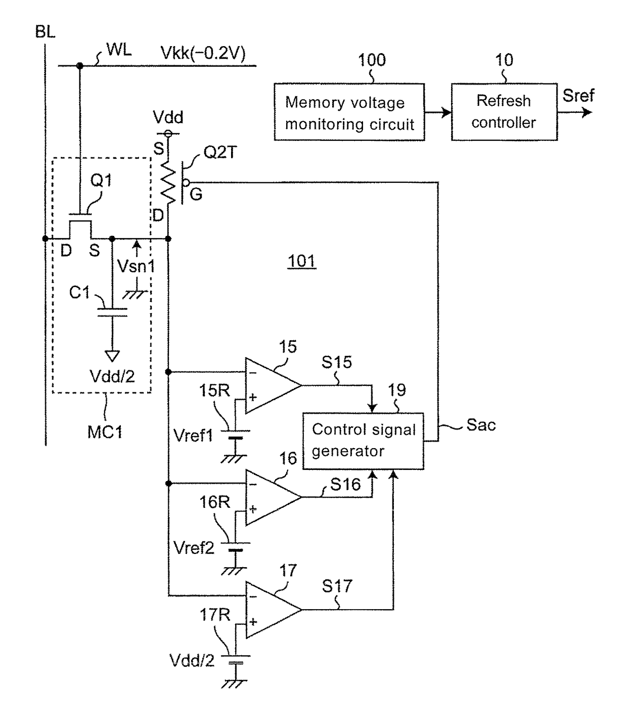
[0082]FIG. 8 is a circuit diagram of a structure example of the refresh control circuit of the memory cell MC1 applied to the DRAM according to the embodiment 2 of the invention. FIG. 9 is an operation timing diagram of the refresh control circuit of FIG. 8. The refresh control circuit of the embodiment 2 is characterized in that besides the memory voltage monitoring circuit 100 of the embodiment 1, the refresh control circuit further includes a refresh control circuit 101, and the refresh control circuit 101 is used for implementing a refresh time longer than that of the conventional example of FIG. 1. The refresh control circuit 101 is a refresh control circuit connected to the general-memorizing memory cell MC1, and includes a thin film transistor (TFT)-type P-channel MOS transistor Q2T disclosed in the non-patent literature 1, comparators 15, 16 and 17, reference voltage sources 15R, 16R, 17R and a control signal generator 19. The comparators 15, 16 and 17 and the control signal...

embodiment

[0093]In the following embodiment, in case of a plurality of memory cells MC1, MC11 of the DRAM, simulation of the inventor and result thereof and voltage setting of the threshold voltage Vref in the embodiment 1 are described below.

[0094]FIG. 10A is an experiment result of the embodiment 1, which illustrates an accumulative distribution of a refresh time Tref. FIG. 10B illustrates a distribution (which is assumed to be a standard distribution) of the memory voltage Vsn with the high level counted after 64 ms of the refresh in case of a high temperature. FIG. 11A illustrates a distribution (which is assumed to be a standard distribution) of the memory voltage Vsn counted after 64 ms of the refresh in case of the high temperature. FIG. 11B illustrates a distribution (which is assumed to be a standard distribution) of the memory voltage Vsn counted after 64 ms of the refresh in case of a room temperature of 20 degrees, etc., i.e. the low temperature. Moreover, FIG. 10A illustrates a s...


PUM


Abstract

A refresh control circuit of a volatile semiconductor memory device is provided, where the volatile semiconductor memory device includes a plurality of memory cells respectively having a select transistor and a memory element, and the refresh control circuit of the volatile semiconductor memory device includes: a first comparison part, which compares a memory voltage of the memory cell of the volatile semiconductor memory device that is different to a general-memorizing memory cell with a specified threshold voltage, and outputs a comparison result signal, and stops self refresh of the memory cell until the memory voltage is decreased to be smaller than the specified threshold voltage. The memory cell is formed in a region adjacent to an array of the general-memorizing memory cell.

Description

CROSS-REFERENCE TO RELATED APPLICATION[0001]This application claims the priority benefit of Japanese application serial no. 2016-030952, filed on Feb. 22, 2016. The entirety of the above-mentioned patent application is hereby incorporated by reference herein and made a part of this specification.BACKGROUND OF THE INVENTION[0002]Field of the Invention[0003]The invention relates to a refresh control circuit and a refresh control method of a volatile semiconductor memory device such as a dynamic random access memory (DRAM), etc., and a volatile semiconductor memory device.[0004]Description of Related Art[0005]FIG. 1 is a circuit diagram of a structure example of a memory cell MC1 of a conventional DRAM and a refresh control circuit. In FIG. 1, a refresh controller 10 and a latch type sense amplifier 11 are included, bit line BL and / BL are connected to the latch type sense amplifier 11, a general-memorizing the memory cell MC1 includes a metal oxide semiconductor (MOS) transistor Q1 and...

Claims


Application Information

Patent Timeline
IPC IPC(8): G11C11/406G11C11/4091
CPCG11C11/40615G11C11/4091G11C11/406G11C11/40626G11C2211/4068H10B12/34H10B12/315
Inventor KIHARA, YUJI
Owner POWERCHIP SEMICON MFG CORP
Why Eureka
Try Eureka